 ALLPCB
Strategic Component Placement: Minimize the Chances of Crosstalk on a PCB
Learn strategic component placement to minimize crosstalk on a PCB. Optimize high-speed signals with expert layout tips for signal integrity.


Learn strategic component placement to minimize crosstalk on a PCB. Optimize high-speed signals with expert layout tips for signal integrity.

Learn PCB component placement strategies with design software for thermal management, high-density layouts, and autorouting at ALLPCB.
Explore advanced PCB routing techniques like differential pair rules and impedance matching with powerful PCB design software at ALLPCB.
Explore advanced PCB routing techniques for multi-layer designs, including stackup, vias, impedance control, and high-density interconnects.
Learn constraint management in PCB design with this beginner's guide. Explore basic rules, software tips, and simple guidelines for success.
Explore when to avoid copper pour in PCB design. Learn about disadvantages, signal coupling, noise issues, and manufacturing problems.

Master high-speed PCB design with tips on signal integrity, impedance matching, crosstalk reduction, and high-frequency materials at ALLPCB.
Learn how PCB copper pour improves signal integrity, thermal management, and design efficiency with this ultimate guide to better PCB layouts.
Learn how strategic thermal pad placement improves PCB reliability, enhances heat dissipation, and extends component lifespan in this guide.
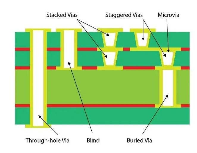
Learn how to select the right vias for PCB design with tips on via types, stitching, size, inductance, and signal integrity for optimal performance.

Learn effective PCB grounding strategies like single point, multi-point, and ground planes in this beginner's guide to quieter layouts.
Learn PCB backdrilling to eliminate via stubs and boost signal integrity in high-speed PCB design with this ultimate guide.

Learn about copper balancing in multilayer PCBs to ensure stability, prevent warping, and maintain signal integrity for optimal performance.
Explore PCB trace impedance, factors, calculations, and control techniques for optimal signal integrity in high-speed designs with ALLPCB.
Learn best practices for through-hole PCB design reliability. Discover tips for robust through-hole design and build a reliable PCB with ALLPCB.
Explore the benefits and challenges of double-sided SMT assembly, including component placement, reflow soldering, and adhesive mounting tips.
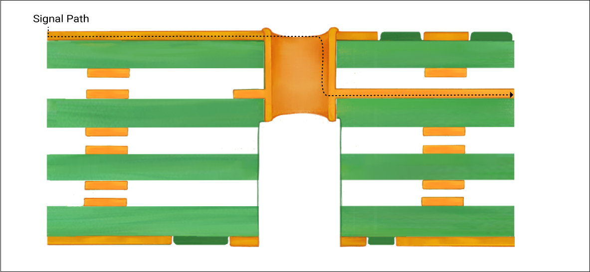
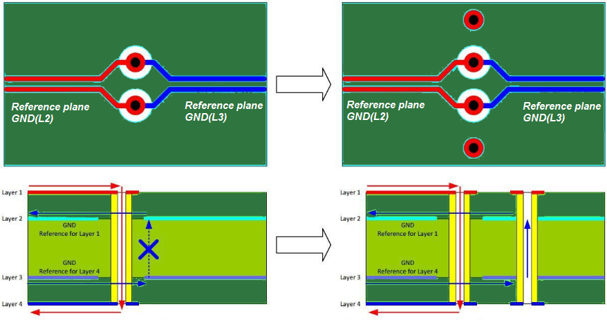
Learn how to avoid cumulative via placement in PCB designs to reduce EMI, improve signal integrity, and prevent plane voids in layers.

Master soldering for PCB assembly with essential tools and techniques. Learn about soldering irons, solder wire, and preventing solder bridges.
Explore advanced PCB layout techniques for high-speed digital circuits, focusing on signal integrity, impedance control, and crosstalk minimization.

Learn how copper pour and thermal relief prevent soldering issues in PCB assembly. A guide to heat dissipation and design tips for engineers.