ALLPCB


When designing a printed circuit board (PCB), one of the key factors that can make or break its performance is thickness. How does PCB thickness affect warpage, and what is the ideal balance to minimize issues? In short, thinner PCBs are more prone to warpage due to reduced structural integrity and sensitivity to thermal stress, while thicker boards offer stability but may increase costs and weight. Finding the sweet spot depends on your design needs, materials, and manufacturing processes. In this blog, we’ll dive deep into the correlation between PCB thickness and warpage, explore challenges with thin PCBs, and discuss solutions like rigid PCB design and board stiffeners to help you achieve optimal results.
Understanding PCB Warpage and Its Causes
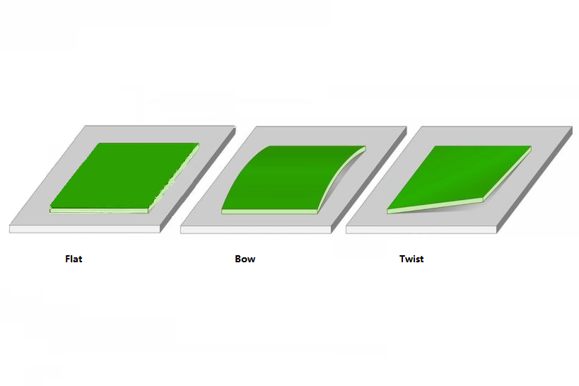
PCB warpage refers to the bending or twisting of a board from its intended flat shape. This deformation can lead to serious issues like poor solder joints, component misalignment, and even complete board failure during assembly or operation. Warpage is often caused by uneven stress during manufacturing, thermal expansion, or material mismatches. But how does thickness play a role in this?
The thickness of a PCB directly impacts its mechanical strength. A thinner board, while lightweight and cost-effective, lacks the rigidity to resist bending under stress. On the other hand, a thicker board can better withstand these forces but may not always be practical for compact designs or budget constraints. Understanding the root causes of warpage—such as coefficient of thermal expansion (CTE) mismatches between layers, improper copper distribution, or rapid cooling during soldering—is crucial for finding the right thickness for your project.
The PCB Thickness Warpage Correlation: Why Thickness Matters
Research and industry studies have shown a clear correlation between PCB thickness and warpage. As PCB thickness decreases, the likelihood of warpage increases. For instance, a board with a thickness of 0.8mm is far more susceptible to bending than one at 1.6mm, which is a standard thickness for many applications. This is primarily due to the reduced structural integrity in thinner boards, making them less capable of resisting mechanical and thermal stresses during manufacturing processes like reflow soldering.
During reflow, temperatures can reach up to 260°C, causing materials in the PCB stack-up to expand at different rates if their CTE values differ. For a thin PCB, this mismatch can easily result in noticeable deformation. According to industry standards like IPC-6012, the maximum allowable warpage for surface-mount boards is typically 0.75% for critical applications. For a 100mm board, this translates to a maximum deviation of just 0.75mm— a tight tolerance that thin boards often struggle to meet.
Conversely, thicker PCBs (e.g., 2.0mm or more) provide greater resistance to warpage due to their enhanced rigidity. However, increasing thickness can lead to higher material costs, added weight, and challenges in applications requiring flexibility or compact designs. Striking a balance is essential, and understanding the specific needs of your project—such as operating environment and component density—can guide you to the optimal thickness.
Thin PCB Challenges: Balancing Cost and Performance
Thin PCBs, often defined as those under 1.0mm in thickness, are popular in modern electronics for their lightweight nature and suitability for compact devices like smartphones and wearables. However, they come with significant challenges that engineers must address to ensure reliability.
1. Increased Warpage Risk
As mentioned earlier, thin PCBs are more prone to warpage due to their reduced ability to handle thermal and mechanical stress. For example, a 0.6mm board undergoing reflow soldering may experience warpage exceeding 1%, far beyond acceptable limits for high-reliability applications.
2. Handling and Assembly Difficulties
Thin boards are fragile and can easily bend or break during handling or automated assembly processes. This fragility often requires specialized equipment or manual care, increasing production time and costs.
3. Component Compatibility Issues
Ball Grid Array (BGA) packages and other high-density components can pose challenges on thin PCBs. The warpage caused by thermal stress can lead to uneven solder joints, resulting in open circuits or reliability issues over time. Studies have shown that warpage in thin boards can cause height variations of up to 0.5mm across the board, making precise component placement difficult.

Rigid PCB Design: Strategies to Minimize Warpage
Rigid PCB design focuses on creating boards with sufficient mechanical strength to resist warpage while meeting electrical and thermal performance requirements. Here are some key strategies to consider when designing rigid PCBs with optimal thickness:
1. Optimize Layer Stack-Up
A balanced layer stack-up is critical to minimizing warpage. Uneven copper distribution across layers can create internal stresses that lead to bending. Aim for symmetry in your design by ensuring that copper layers on the top and bottom halves of the board are as similar as possible in thickness and coverage. For a 4-layer board at 1.6mm thickness, a common stack-up might include signal layers on the outer sides with ground and power planes in the middle, maintaining a balanced structure.
2. Choose the Right Materials
Material selection plays a huge role in warpage control. High-Tg (glass transition temperature) materials, with Tg values above 170°C, are less likely to deform under heat compared to standard FR-4 materials with Tg around 130°C. Additionally, selecting materials with similar CTE values for the core and prepreg layers can reduce thermal mismatch during manufacturing.
3. Control Manufacturing Processes
Warpage often occurs during cooling after high-temperature processes like reflow. Gradual cooling, rather than rapid quenching, can help reduce internal stresses in the board. Working closely with your manufacturing partner to optimize process parameters—such as temperature profiles and panelization techniques—can significantly improve board flatness.
Board Stiffeners: A Solution for Warpage in Thin and Rigid PCBs
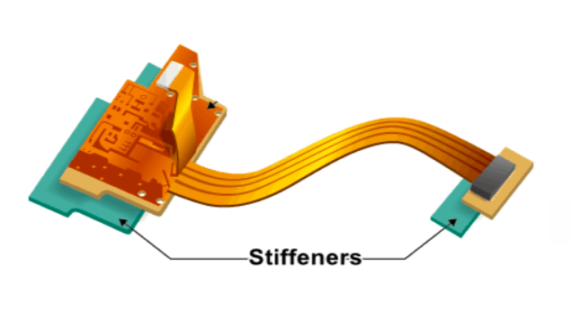
For designs where thin PCBs are necessary, or where warpage remains a concern despite optimized thickness, board stiffeners offer a practical solution. Stiffeners are additional mechanical supports added to the PCB to enhance rigidity without altering the core electrical design.
What Are Board Stiffeners?
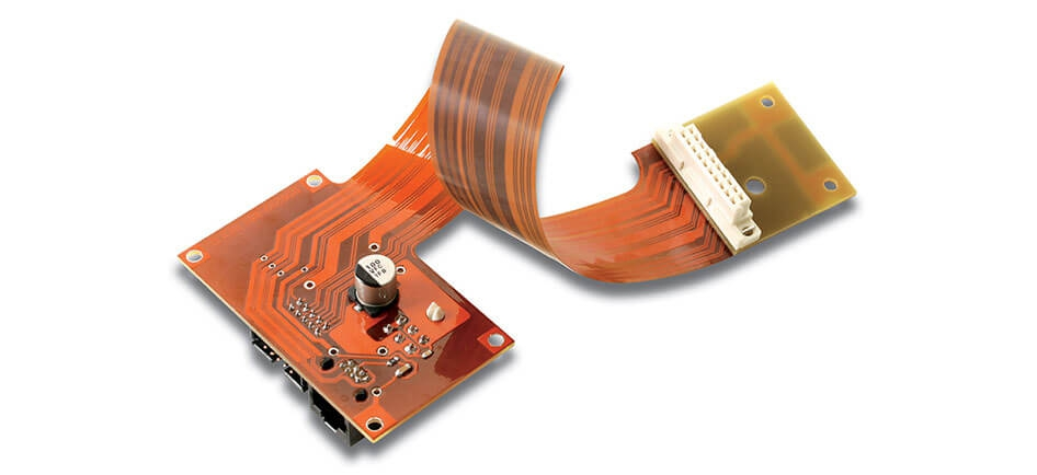
Board stiffeners are typically made from materials like FR-4, polyimide, or metal (e.g., aluminum) and are attached to specific areas of the PCB to prevent bending. They are commonly used in flex and rigid-flex designs but can also be applied to rigid PCBs to address warpage in critical areas, such as under heavy components or connectors.
Benefits of Using Stiffeners
Stiffeners provide several advantages, including:
- Enhanced Mechanical Support: They prevent bending in thin PCBs, maintaining flatness during assembly and operation.
- Improved Component Reliability: By reducing warpage, stiffeners help ensure proper solder joint formation for components like BGAs.
- Cost-Effective Solution: Adding a stiffener can be more economical than increasing overall board thickness, especially for localized warpage issues.
Placement and Design Tips
When incorporating stiffeners, consider their placement carefully. They should be positioned in areas prone to stress, such as near heavy components or along the edges of the board. Ensure that stiffeners do not interfere with electrical traces or component placement. For instance, a 0.2mm polyimide stiffener added to a 0.8mm PCB can reduce warpage by up to 50%, based on industry case studies, without adding significant weight.
Finding the Sweet Spot: Balancing Thickness and Design Needs
So, what is the ideal PCB thickness to minimize warpage while meeting design requirements? Unfortunately, there’s no one-size-fits-all answer. However, here are some guidelines based on common applications:
- Standard Applications: A thickness of 1.6mm is often considered the sweet spot for many rigid PCBs. It provides a good balance of rigidity, cost, and manufacturability while keeping warpage within acceptable limits (typically under 0.75% as per IPC standards).
- Compact Devices: For thinner designs (e.g., 0.8mm to 1.0mm), consider using high-Tg materials and stiffeners to mitigate warpage risks.
- High-Power Applications: Thicker boards (2.0mm or more) may be necessary for applications with high thermal loads or heavy components, as they offer better stability and heat dissipation.
Ultimately, the sweet spot depends on a combination of factors: your budget, the complexity of the design, the operating environment, and the manufacturing capabilities at your disposal. Simulation tools can also help predict warpage based on thickness and material choices, allowing you to fine-tune your design before production.
Practical Tips for Engineers to Minimize Warpage
To wrap up, here are some actionable tips to help you manage PCB thickness and warpage effectively:
- Simulate Early: Use thermal and mechanical simulation software to predict warpage risks based on your chosen thickness and materials.
- Collaborate with Manufacturers: Work closely with your fabrication partner to understand their process limitations and optimize panelization or cooling methods.
- Test Prototypes: Build and test prototypes at your target thickness to identify warpage issues before full-scale production.
- Consider Stiffeners: For thin or high-risk designs, integrate stiffeners strategically to reinforce weak areas without increasing overall thickness.
- Monitor Copper Balance: Ensure even copper distribution across layers to avoid internal stresses that contribute to warpage.
Conclusion: Achieving Flatness Through Smart Design
The impact of PCB thickness on warpage is undeniable, with thinner boards facing higher risks due to reduced rigidity and thermal sensitivity. By understanding the PCB thickness warpage correlation, addressing thin PCB challenges, leveraging rigid PCB design strategies, and incorporating solutions like board stiffeners, engineers can find the sweet spot that balances performance, cost, and reliability. Whether you’re designing for a compact wearable or a high-power industrial system, taking a proactive approach to thickness and warpage control will ensure your PCBs meet the highest standards of quality and functionality.