ALLPCB


Introduction
Building a DIY audio amplifier on a double-sided PCB offers electronic hobbyists a rewarding project that combines circuit design with hands-on fabrication skills. This amplifier project electronics setup allows you to amplify weak audio signals from sources like microphones or media players into powerful output for speakers. Double-sided PCBs provide more routing flexibility than single-sided boards, enabling better separation of signal paths and ground planes to minimize noise. Hobbyists appreciate this approach because it results in cleaner sound reproduction and a compact layout suitable for enclosures. In this step-by-step guide, you will learn everything from schematic planning to final testing, tailored for home workshops.
Why Build a DIY Audio Amplifier on a Double-Sided PCB?
A double-sided PCB guide reveals advantages like increased component density and improved electrical performance for audio circuits. Single-sided boards limit trace routing, often forcing long paths that pick up interference, but double-sided designs dedicate one layer to signals and the other to ground, reducing crosstalk. This matters for audio amplifier PCBs because low-level signals are sensitive to hum and distortion from power lines. Hobbyists gain practical experience in via usage and layer alignment, skills transferable to more complex builds. Moreover, double-sided boards support star grounding schemes, where ground returns converge at one point, essential for low-noise operation. Overall, this format elevates a simple DIY amplifier into a professional-sounding device.
Fundamentals of Audio Amplifier Circuits
Audio amplifiers boost small input signals while preserving waveform fidelity across the audible frequency range. A typical hobbyist design includes an input stage for coupling, a gain stage using transistors, and an output stage for driving speakers. Feedback loops stabilize gain and reduce distortion by comparing output to input. Power supply decoupling prevents ripple from modulating the audio signal. Transistors operate in class AB mode for efficiency, balancing linearity and heat dissipation. Understanding these blocks ensures your PCB layout supports optimal current paths and thermal flow.
Key PCB Design Principles for Low-Noise Audio Amplifiers
Effective PCB layout begins with component placement to shorten high-impedance signal traces and isolate them from power rails. Place input jacks near the preamp section and output transistors near speaker terminals to minimize loop areas that induce noise. Implement a ground plane on the bottom layer, connected via multiple vias to component grounds, forming a low-impedance return path. Decoupling capacitors should sit close to transistor bases and collectors, with short, wide traces to supply pins. Follow IPC-2221 guidelines for trace widths to handle current without excessive voltage drop, especially in output stages. Separate analog ground from power ground until a single star point to avoid injecting digital noise, though this DIY amplifier focuses on analog purity.
Related Reading: Signal Integrity in Audio Amplifier PCBs: Routing Techniques for Crystal Clear Sound
Step-by-Step Guide: Designing the Schematic
Start with a basic schematic featuring coupling capacitors at input and output to block DC. Use small-signal transistors for voltage amplification, followed by push-pull power transistors biased for class AB operation. Include bias resistors to set quiescent current and feedback resistors for gain control. Add electrolytic capacitors for power supply filtering and ceramic types for high-frequencyf bypass. Zobel networks at the output stabilize the load interaction. Draw the netlist clearly, verifying connections with a simulator if available, to catch errors before layout.
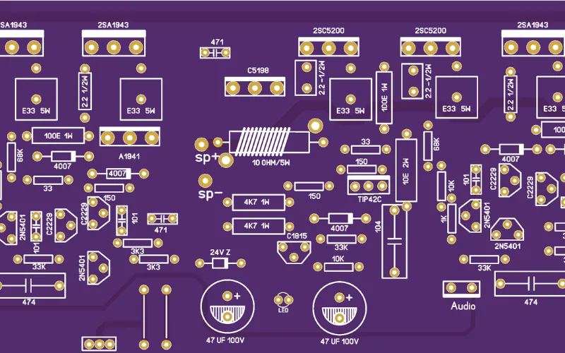
Transferring to Double-Sided PCB Layout
Choose a board size fitting your enclosure, around credit-card dimensions for portability. Place components on the top layer, routing sensitive audio traces there while using the bottom for ground pour and power distribution. Position heat-generating transistors near board edges for heatsink mounting, with thermal vias under collectors if needed. Route input signals first, keeping them away from output paths to prevent oscillation. Use vias sparingly but effectively for layer jumps, plating them adequately during fabrication. Pour copper on unused bottom areas as ground plane, stitching with vias every few millimeters for uniformity.
Adhering to IPC-6012 performance specifications ensures the board withstands thermal stresses during operation. Double-check clearances between high-voltage traces and ground to prevent arcing.
Related Reading: Designing a Low-Noise Audio Amplifier PCB: Minimizing Ground Loops and Interference
Fabricating the Double-Sided PCB at Home
Print your layout mirrored for the bottom layer on transparency film using a laser printer for sharp toner. Expose both sides of photosensitive copper-clad board to UV light through the films, aligning layers precisely with registration holes. Develop in sodium carbonate solution, then etch in ferric chloride, agitating for even copper removal. Double-sided alignment requires a jig or tape to prevent slippage during exposure. Drill vias after etching, using a fine bit for clean holes. Inspect for shorts or opens under magnification, cleaning residue with isopropyl alcohol.
Assembling the Components
Solder through-hole components starting with low-profile resistors and capacitors, forming good fillet joints per J-STD-001 requirements for reliability. Mount transistors with insulators if heatsinks are used, applying thermal compound sparingly. Install electrolytic capacitors observing polarity, and trim leads flush to avoid shorts. Socket sensitive parts if prototyping allows easy swaps. Reflow solder joints with a torch or iron at controlled temperature to avoid cold joints. Final clean with flux remover ensures no corrosive residues remain.
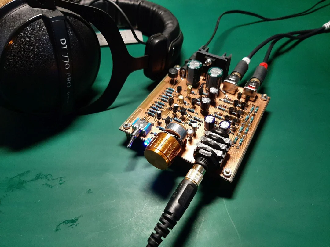
Testing and Tuning Your Amplifier
Power up with a current-limited supply, measuring quiescent current at the output stage for proper bias. Inject a sine wave at input, scoping output for distortion-free amplification across frequencies. Check for oscillation by monitoring with a spectrum analyzer or listening for whistles. Adjust bias if output is clipped or crossover distortion appears. Load with a resistor simulating speaker impedance, verifying maximum output swing. Enclose in a shielded box to further reduce external interference.
Troubleshooting Common Issues in DIY Amplifiers
Noise pickup often stems from unshielded input traces or poor grounding; revisit the star point and add shielding. Distortion arises from insufficient decoupling or bias drift, addressed by larger filter caps or temperature-stable resistors. Overheating indicates inadequate heatsinking or bias excess, monitored with a thermometer. Board warpage from uneven etching affects soldering; flatten with weights during cure. Parasitic oscillation from long leads requires damping resistors in series with bases. Systematic voltage checks isolate faults quickly.
Conclusion
This double-sided PCB guide equips electronic hobbyists to build a reliable audio amplifier PCB from concept to operation. Key takeaways include prioritizing signal integrity through layered routing, adhering to standards like IPC-A-600 for visual acceptability, and methodical testing. The project fosters skills in layout, fabrication, and debugging applicable to future endeavors. Enjoy the satisfaction of custom sound amplification tailored to your needs. Experiment further by scaling power or adding tone controls.
FAQs
Q1: What makes a double-sided PCB ideal for a DIY amplifier project?
A1: Double-sided boards allow separate signal and ground planes, reducing noise in audio amplifier PCBs. Hobbyists route delicate inputs on top and pour solid ground on bottom, minimizing loops. Vias connect layers efficiently without crowding. This setup follows basic IPC principles for performance, yielding clearer sound than single-sided alternatives. Overall, it balances complexity with home fabrication ease.
Q2: How do I avoid noise in my hobbyist audio amplifier PCB?
A2: Implement star grounding where all returns meet at one via near the power input. Keep signal traces short and twisted with grounds. Place decoupling capacitors within millimeters of transistors. Separate power traces from audio paths on the double-sided layout. Test iteratively with an oscilloscope for hum rejection.
Q3: What are essential steps in a double-sided PCB guide for amplifiers?
A3: Begin with schematic verification, then layout prioritizing input-to-output flow. Align layers precisely during exposure for vias. Etch evenly, drill, and inspect per acceptability criteria. Solder methodically, testing subsections. This ensures a functional electronics amplifier project.
Q4: Can beginners handle assembly for an audio amplifier PCB?
A4: Yes, with through-hole parts and basic tools, following soldering best practices. Start with resistors, progress to transistors. Check continuity after each stage. Common pitfalls like cold joints are fixed by reheating. Results rival commercial boards for hobbyist use.
References
IPC-2221B — Generic Standard on Printed Board Design. IPC, 2003
IPC-6012E — Qualification and Performance Specification for Rigid Printed Boards. IPC, 2015
IPC J-STD-001G — Requirements for Soldered Electrical and Electronic Assemblies. IPC, 2017
IPC-A-600H — Acceptability of Printed Boards. IPC, 2019