ALLPCB


Introduction
Electric engineers designing power electronics face unique challenges when dealing with high currents, where standard PCBs fall short in thermal dissipation and mechanical integrity. Heavy copper double-sided PCBs address these needs by incorporating thicker copper layers on both sides of the board, typically starting from 3 ounces per square foot or more. This construction allows for robust current handling in compact form factors, making them ideal for applications like power supplies and motor drives. The enhanced copper thickness reduces resistance and voltage drop, while improving heat spreading across the board. As power densities increase in modern electronics, understanding heavy copper double-sided PCB technology becomes essential for reliable power PCB design. This article delves into their definition, design principles, manufacturing processes, and practical applications.
What Are Heavy Copper Double-Sided PCBs and Why Do They Matter?
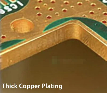
Heavy copper double-sided PCBs feature copper foil thicknesses greater than the standard 1 or 2 ounces per square foot, often ranging from 4 to 10 ounces or higher on both the top and bottom layers. Unlike conventional double-sided boards used for signal routing, these prioritize power delivery with wide traces capable of carrying tens or hundreds of amperes. The term "heavy copper" lacks a strict IPC definition but is industry-accepted for boards exceeding 3 ounces per square foot, enabling high-current double-sided PCB configurations. They matter because they support the shift toward compact, high-power systems in sectors like renewable energy and industrial automation, where space constraints demand integrated power and control circuitry. Engineers benefit from their ability to minimize the need for external bus bars or heatsinks in many cases. Ultimately, heavy copper double-sided PCBs bridge the gap between performance and size in demanding electrical environments.
Design Principles for Thick Copper PCBs in High-Current Applications
Power PCB design for heavy copper double-sided boards begins with calculating trace widths based on expected current loads and allowable temperature rise. The IPC-2152 standard provides charts and formulas accounting for copper thickness, trace length, and board stacking to determine safe current-carrying capacities, superseding older IPC-2221 guidelines. For instance, thicker copper allows narrower traces for the same current compared to 1-ounce material, but engineers must factor in plating uniformity and etch factors. Spacing between traces increases with copper weight to prevent shorting during etching, typically requiring 10 to 20 mils more than standard boards. Vias and through-holes demand larger diameters to handle current without necking down during plating. Layer-to-layer alignment is critical on double-sided heavy copper PCBs to avoid registration issues under thermal stress.
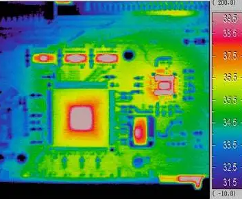
Thermal management drives many design choices, as thicker copper alters the coefficient of thermal expansion mismatch with the substrate. Engineers simulate heat flow using finite element analysis to predict hotspots, ensuring junctions stay below critical thresholds. Copper balancing between top and bottom layers minimizes warpage, a common issue in thick copper PCB fabrication. Signal integrity remains secondary but requires careful routing to avoid crosstalk from power planes. Adhering to these principles ensures the board meets performance specs under sustained high-current operation.
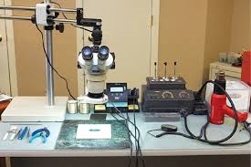
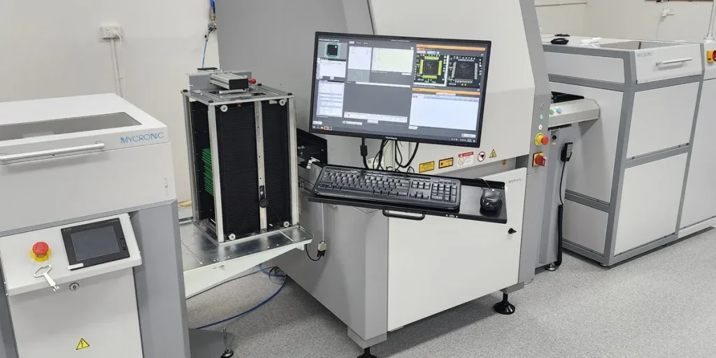
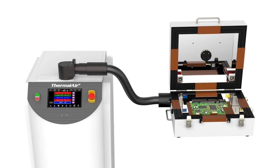
Manufacturing Processes for Heavy Copper Double-Sided PCBs
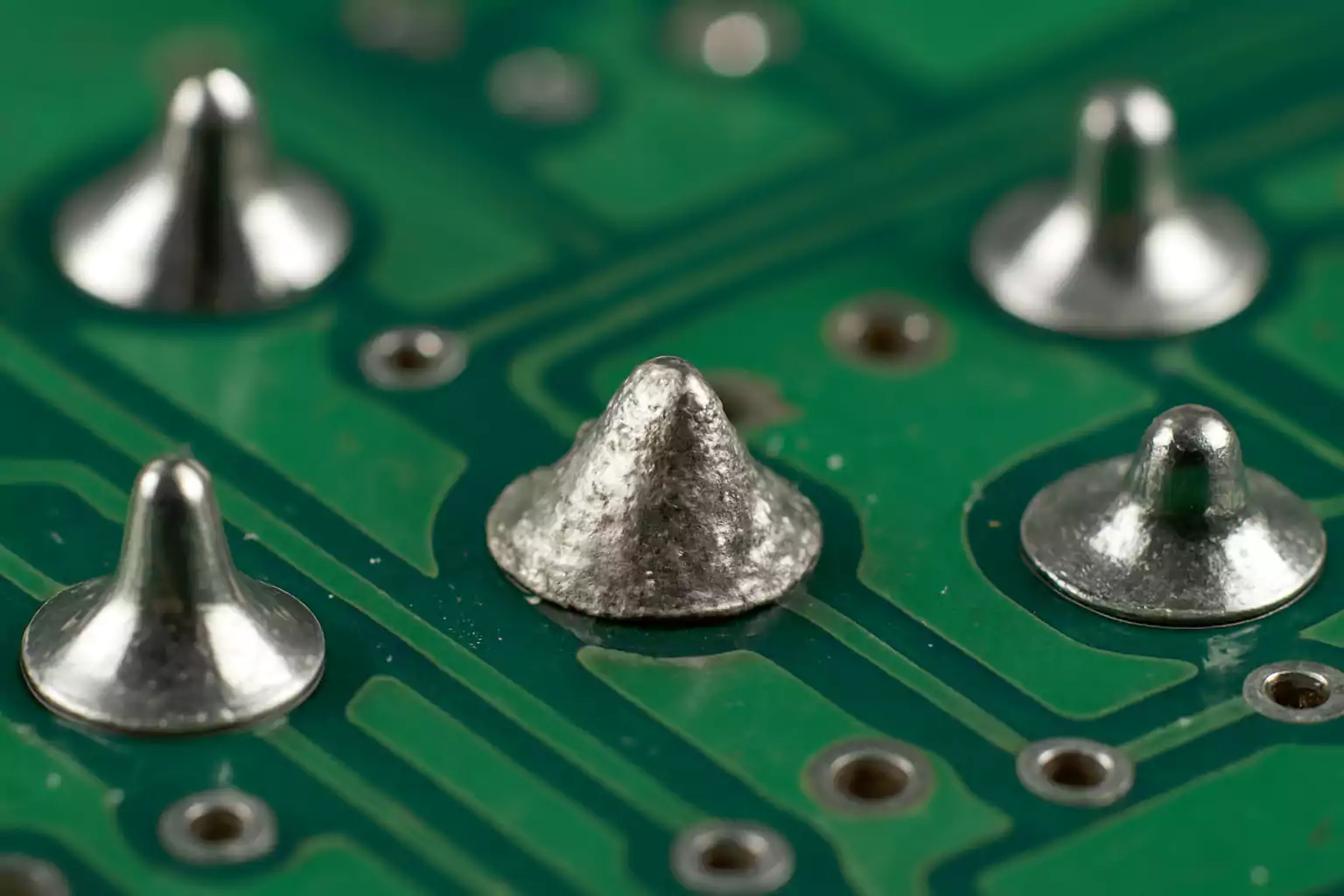
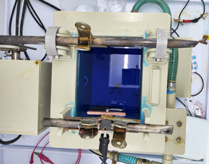
Fabricating thick copper PCBs involves specialized techniques to achieve uniform plating and precise etching. Manufacturers start with heavy copper-clad laminates, then use panel electroplating to build additional copper thickness on both sides, often reaching 4 to 6 ounces total. Differential etching compensates for the trapezoidal profile of thick traces, where the top etches faster than the bottom, ensuring consistent widths. This process demands controlled chemistry to prevent undercutting or over-etching, which could compromise current capacity. Lamination uses high-Tg resins to withstand the stresses of heavy copper deposition and drilling.
Drilling and plating present additional hurdles due to the rigidity of thick copper stacks. Larger drill bits and peck drilling sequences prevent bit breakage and burrs on double-sided boards. Solder mask application requires thicker formulations to cover tall traces without voids, followed by surface finishes like ENIG for solderability in power applications. Final inspection per IPC-A-600 verifies conductor geometry, plating thickness, and board flatness. These steps ensure high-current double-sided PCBs deliver consistent quality from prototype to production.
Applications of Heavy Copper Double-Sided PCBs
In double-sided PCB power supplies, heavy copper layers serve as integrated bus structures, distributing high currents to converters and rectifiers efficiently. Automotive inverters benefit from their compact footprint, handling peak loads from electric motors without bulky wiring harnesses. Industrial welding equipment relies on thick copper PCBs for precise current control, where rapid thermal cycling demands robust construction. Renewable energy systems, such as solar inverters, use these boards to manage DC-to-AC conversion at kilowatt levels.
Defense and aerospace power modules also adopt high-current double-sided PCBs for their vibration resistance and high reliability. In each case, the design reduces assembly complexity by embedding power paths directly into the board. Engineers select copper weights based on duty cycles and ambient conditions to optimize system efficiency.
Related Reading: Heavy Copper PCBs: A Comprehensive Guide for High-Power Applications
Best Practices and Challenges in Power PCB Design
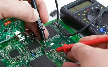
Effective power PCB design incorporates symmetric copper distribution to combat warpage during reflow soldering. Pre-baking boards mitigates moisture absorption in thick laminates, aligning with IPC-6012 performance qualifications. Engineers specify extended cure cycles for solder masks over heavy traces to prevent cracking. Testing includes thermal cycling and high-current burn-in to validate real-world performance.
Common challenges include via reliability under thermal expansion and edge connector plating uniformity. Solutions involve filled vias or stitched arrays for current sharing, plus beveling panel edges during fabrication. Collaboration between design and manufacturing teams early in the process avoids costly iterations. These practices ensure heavy copper double-sided PCBs excel in demanding high-current environments.
Related Reading: Heavy Copper PCB Design: Overcoming Thermal Challenges
Conclusion
Heavy copper double-sided PCBs stand out for their ability to power high-current applications through superior current handling and thermal performance. Key to success lies in precise design per IPC-2152, meticulous manufacturing, and adherence to standards like IPC-A-600 and IPC-6012. Electric engineers can leverage these boards to create efficient, compact systems for power electronics. By addressing challenges like warpage and plating uniformity, they unlock reliable operation in critical sectors. As demands for higher power densities grow, thick copper PCB technology will remain a cornerstone of advanced power PCB design.
FAQs
Q1: What defines a heavy copper double-sided PCB?
A1: A heavy copper double-sided PCB uses copper thicknesses exceeding 3 ounces per square foot on both layers, optimized for high-current double-sided PCB needs. This construction supports power-intensive traces while maintaining double-sided routing flexibility. Design focuses on current capacity charts from IPC-2152 to ensure safe operation. Manufacturing employs panel plating for uniformity.
Q2: How does thick copper improve power PCB design?
A2: Thick copper in power PCB design boosts current-carrying capacity, reduces I^2R losses, and enhances heat dissipation across the board. It allows narrower traces for the same amperage compared to standard copper, aiding compact layouts. Engineers calculate widths using temperature rise limits to prevent hotspots. Applications like double-sided PCB power supplies benefit from integrated bussing.
Q3: What manufacturing challenges arise with high-current double-sided PCBs?
A3: High-current double-sided PCBs face issues like differential etching and warpage due to asymmetric copper. Solutions include balanced layering and high-Tg materials per IPC-6012 guidelines. Plating buildup requires precise control to avoid voids. Inspection verifies trace profiles against IPC-A-600 criteria.
Q4: Why choose heavy copper for high-current applications?
A4: Heavy copper excels in high-current applications by handling elevated amperages without excessive heating or voltage drop. It simplifies assembly by replacing discrete power components with board-integrated paths. Reliability improves under thermal stress, suiting power electronics. Standards ensure consistent performance across production runs.
References
IPC-2152 — Standard for Determining Current Carrying Capacity in Printed Board Design. IPC, 2009
IPC-6012E — Qualification and Performance Specification for Rigid Printed Boards. IPC, 2017
IPC-A-600K — Acceptability of Printed Boards. IPC, 2020