ALLPCB


If you're designing printed circuit boards (PCBs) for ultrasound systems, you might be wondering how to optimize component placement for efficient signal routing. The answer lies in strategic planning: prioritize critical signal paths, separate analog and digital components, and minimize trace lengths for high-speed signals. In this comprehensive guide, we'll dive deep into the best practices for PCB component placement in ultrasound applications, explore techniques like shortest path routing on PCBs, and discuss the importance of critical signal routing, analog and digital separation, and mixed signal PCB layout to ensure top performance.
Why Component Placement Matters in Ultrasound PCBs
Ultrasound systems rely on precise signal integrity to produce accurate imaging or therapeutic results. These devices handle high-frequency signals, often in the range of 1 to 20 MHz, where even small delays or interference can degrade performance. Poor component placement can lead to longer signal paths, increased noise, and electromagnetic interference (EMI), all of which compromise the system's reliability. By optimizing placement, you can achieve shorter trace lengths, reduce crosstalk, and ensure clean signal transmission, which is vital for both diagnostic and therapeutic ultrasound equipment.
Key Principles of PCB Component Placement for Ultrasound Systems
Let’s break down the core strategies for effective component placement in ultrasound PCBs. These principles focus on minimizing signal distortion and maximizing efficiency.
1. Prioritize Critical Signal Paths
In ultrasound PCBs, certain signals, such as those from transducers or high-speed data lines, are more sensitive to delays and noise. These are often referred to as critical signal routing on PCBs. To optimize their paths, place related components as close together as possible to reduce trace lengths. For instance, position the transducer interface components near the analog front-end (AFE) circuitry to keep signal paths under 10-15 mm if feasible. Shorter paths lower the risk of signal degradation and reduce parasitic inductance, which can impact signals at frequencies above 5 MHz.
Additionally, use shortest path routing on PCBs by planning direct connections without unnecessary vias or sharp bends. Each via can introduce a delay of around 0.1 to 0.5 ns, so minimizing them is key in high-frequency designs like ultrasound systems.
2. Separate Analog and Digital Sections
Ultrasound PCBs often combine analog and digital signals, making analog and digital separation on PCBs a critical design aspect. Analog signals, such as those from the transducer, are highly sensitive to noise from digital circuits like microcontrollers or data converters. To prevent interference, physically separate these sections on the board. Allocate distinct zones for analog and digital components, and ensure their ground planes are split but connected at a single point to avoid ground loops.
For example, place the analog components on the left side of the PCB and digital components on the right, with a clear boundary between them. Route analog traces away from high-speed digital lines to avoid crosstalk, which can introduce noise levels as high as 50 mV in sensitive circuits.
3. Optimize for Mixed Signal PCB Layout
Designing a mixed signal PCB layout requires balancing the needs of both analog and digital circuits while maintaining signal integrity. Beyond physical separation, consider the power supply routing. Use separate voltage regulators for analog and digital sections to prevent noise from digital switching (often at 100 kHz or higher) from coupling into the analog power lines. Additionally, place decoupling capacitors (typically 0.1 μF to 1 μF) close to the power pins of each IC to filter out high-frequency noise.
Another tip is to route sensitive analog traces on inner layers if you're using a multilayer board. This shields them from external EMI and digital noise, which is especially important in ultrasound systems where signal amplitudes can be as low as 1 mV.
Advanced Techniques for Signal Routing in Ultrasound PCBs
Once components are placed strategically, the next step is routing the signals efficiently. Here are some advanced techniques tailored for ultrasound applications.
1. Implement Shortest Path Routing Strategies
As mentioned earlier, shortest path routing on PCBs is essential for high-frequency signals. Use design software with autorouting features to find the most direct paths, but manually adjust critical traces to ensure they avoid noisy areas. For instance, a signal trace running at 10 MHz can experience significant attenuation if it exceeds 20-30 mm in length due to parasitic capacitance. Keep these traces short and straight, and avoid 90-degree bends, which can cause signal reflection. Instead, use 45-degree angles or smooth curves for better signal flow.
2. Manage Impedance for Critical Signal Routing
For critical signal routing on PCBs, maintaining controlled impedance is crucial. Ultrasound signals often require a specific characteristic impedance, typically 50 ohms for RF lines, to prevent signal loss. Calculate the trace width and spacing based on the PCB stack-up and dielectric constant (often around 4.5 for FR-4 material). For a 50-ohm trace on a standard 1.6 mm thick board, the width might be around 0.3 mm with a ground plane directly beneath it. Use simulation tools to verify impedance before manufacturing to avoid costly redesigns.
3. Minimize Crosstalk and EMI
Crosstalk between adjacent traces can distort ultrasound signals, especially in densely packed PCBs. Maintain a spacing of at least 3 times the trace width (3W rule) between high-speed lines to reduce coupling. For example, if your trace width is 0.2 mm, keep a 0.6 mm gap between parallel traces. Additionally, route high-frequency traces over a continuous ground plane to provide a low-impedance return path, reducing EMI by up to 20-30% compared to split or incomplete ground planes.
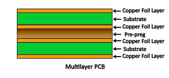
Layer Stack-Up Considerations for Ultrasound PCBs
Ultrasound PCBs often require multilayer designs (4 to 8 layers) to accommodate complex routing and shielding needs. A typical stack-up might include:
- Top Layer: Component placement and critical signal traces
- Layer 2: Ground plane for shielding and return paths
- Layer 3: Power distribution or additional signal routing
- Bottom Layer: Secondary components or low-speed signals
Dedicate internal layers to ground and power planes to minimize noise. For instance, placing a ground plane between two signal layers can reduce crosstalk by up to 40% in high-frequency designs. Ensure vias are used sparingly, as each via can add 1-2 ohms of resistance and affect signal timing.
Thermal Management in Component Placement
Ultrasound systems often generate heat, especially in power-intensive components like amplifiers or transducers. Poor thermal management can lead to signal drift or component failure. Place heat-generating components away from sensitive analog circuits to prevent thermal noise, which can introduce errors of 0.5-1 mV in low-level signals. Use thermal vias or heat sinks near high-power components to dissipate heat, keeping junction temperatures below 85°C for most ICs.
Design Tools and Simulation for Optimization
Modern PCB design tools offer features to simulate signal integrity, impedance, and EMI before fabrication. Use these tools to test different component placements and routing scenarios. For example, simulate a 5 MHz ultrasound signal to check for reflections or delays, adjusting trace lengths to match within 1-2 mm for differential pairs. These simulations can save hours of rework by identifying issues like crosstalk or impedance mismatches early in the design phase.
Common Mistakes to Avoid in Ultrasound PCB Design
Even experienced engineers can overlook small details that impact performance. Here are some pitfalls to watch out for:
- Overcrowding Components: Packing components too closely can lead to thermal issues and routing challenges. Leave at least 1-2 mm spacing around high-power parts.
- Ignoring Ground Planes: A broken or poorly designed ground plane can increase EMI by 30-50%. Ensure a continuous plane under critical traces.
- Neglecting Decoupling: Failing to place decoupling capacitors near ICs can introduce noise spikes of 100 mV or more during switching.
Conclusion: Achieving Excellence in Ultrasound PCB Design
Optimizing PCB component placement for ultrasound systems is a balancing act of signal integrity, noise reduction, and thermal management. By focusing on shortest path routing on PCBs, prioritizing critical signal routing, ensuring analog and digital separation, and following best practices for mixed signal PCB layout, you can create designs that deliver reliable performance in demanding applications. Whether you're working on medical imaging devices or industrial ultrasound equipment, these strategies will help you minimize delays, reduce noise, and improve overall efficiency.
Start by planning your layout with critical paths in mind, use simulation tools to validate your design, and always consider the unique requirements of high-frequency signals. With careful attention to detail, your ultrasound PCBs can achieve the precision and reliability needed for cutting-edge technology.