My Message
 Suggestions


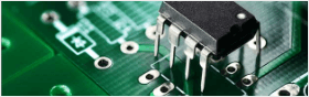
Description: Blind holes and buried holes are applied to high-density boards. Engineers use this design to save the space of the boards, so that to reduce the volume of the boards. For example, cellphone PCBs.
Clarification:
(1) Laser Drilling
Why should we use laser drilling? First, because customers want us to do the laser drilling. Second, because the hole size of the blind hole is less than 6mil, only laser drilling can achieve this. Third, there are blind holes between layer 1 and layer 2 and there are buried holes between layer 2 and layer 3. So we need to use laser drilling.
So what is the theory of laser drilling? Laser drilling will gasify or melt the board to form holes by absorbing board heat. Thus, the board must be optical absorptive. Usually, it will be RCC material, which will not be reflective because of non-glass cloth in it.
Here, let me introduce RCC material to you. RCC means resin coated copper foil, which can be formed by covering a special resin on the surface of the copper foil. There are three main suppliers of RCC material: SYE, Mitsui and LG. Thickness of the resin are 50, 65, 70, 75 , 80um. Thickness of copper foil are 12, 18um. There are RCC with high TG value and RCC with low TG value. The dielectric constant is lower than that of FR-4.
What should we prepare to finish laser drilling? It is very hard for laser to through the copper, we need to etch Cu clearance, which size will be the same as that of blind hole. We need to make mark point of laser drilling on L2/LN-1 layer and we need to add remarks in the film. To etch blind and buried holes, we must use LDI.
Process of production. We follow customer’s layer sort to arrange the layers. Then we follow below process: drill LDI tooling holes- dry film - etching blind holes - laser drilling - drill through holes - PTH Production.

(2) Mechanical Blind Holes/Buried Holes.
It can be used when the size of bit is over 0.2mm. Under normal circumstances, we can only do panel plating for once and pattern plating for one time to any copper. If the width of outer trace is over 6mil and through holes thickness is less than 80mil, and we can do panel plating for the blind holes. If the width of outer trace is over 6mil but through holes thickness is more than 80mil, when we do blind hole plating, we need to add film on the board. If the width of outer trace is less than 6mil and through holes thickness is over 80mil, when we do blind hole plating, we should also add film on the board.
How to add film? When the aspect ratio of blind hole is less than 0.8(L/D), we need to do exposure to the outer panel with film and do panel plating to the blind holes in inner layers. When the aspect ratio of blind hole is over 0.8(L/D), we need to do exposure to the outer panel with film and we also need to do plating exposure film or LDI exposure. At the same time, we do panel plating to the blind holes in inner layers.
How to do blind hole exposure? When the size of blind hole is less than 0.4mm(16mil), we use LDI to expose blind holes. When the size of blind hole is over 0.4mm(16mil), we use film to expose blind holes. How to add film to buried holes? When the trace width is less than 4 mil, we need add film to do exposure to buried holes. When the trace width is over 4 mil, we just do panel plating to the whole board with buried holes.

(3) Some Special Notes for Boards with Blind Holes or Buried Holes.
a. Resin plugged blind holes. When there are many large buried holes in the board, we need to plug much resin to avoid board thickness changing.
b. When there are blind holes in the outer layer, we need to follow the process: Press boards - remove glue - drill holes - plated through holes - panel planting - dry film - pattern plating.
c. Because of the complexity of doing blind holes and buried holes, please keep the distance between trace to board outline to 0.8 inches.