My Message
 Suggestions


With the development of new electronic devices, components are getting smaller and smaller, and the demand is increasing. Not surprisingly, miniaturization and ever-increasing power and cooling requirements have significantly increased the frequency of voids, especially at the bottom of the bottom-end device (BTC) such as the quad flat no-lead device (QFN). At present, the call for mitigating this defect is getting louder and louder, and some manufacturers even explicitly specify that the hole rate under the ground plane should be as close as possible to zero.
Automated X-ray Inspection (AXI) equipment uses X-rays to penetrate PCB boards and acquire images on dedicated imaging sensors, which realizes the perspective of PCB boards and solves the quality control of component packaging such as BGA and CSP. problem. According to the needs, AXI can be designed into 2D/3D. Because the solder joint contains an alloy of lead and tin which can absorb a large amount of X-rays, it is irradiated in comparison with X-rays passing through other materials such as glass fiber, copper and silicon. The X-rays on the dots are absorbed in a large amount to form a black image, and then the solder joint defects can be automatically verified by image analysis calculation.
The question is how to alleviate what you can't even see? X-ray analysis can be used to measure voids in electronic components. However, there are many different settings and parameters to consider before making a successful measurement. This article will outline how different X-ray settings will affect the final analysis quality. Comprehensive guide to X-ray inspection.

Introduction:
X-ray analysis has had an interesting history. In 1895, German physicist Wilhelm Conrad Rontgen stumbled upon X-rays. At the time, he did not understand his findings at all, and for reasons unknown, he called it X-rays. X-ray has rapidly developed to the present day and has been widely used in the fields of medical treatment, transportation, food and beverage, and electronics industry.
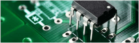
In the electronics industry, X-rays have become a hot topic after the emergence of ball grid array (BGA) components (Figure 1). There are two opposing views on whether a void is a defect:
1) The void is the cause of the crack, which causes the solder joint to fail.
2) Cavities can prevent cracks from preventing failure.
Cavities can cause field failures, reliability issues, and thermal issues with electronic components. It can be said that it is one of the biggest challenges of PCB assembly today. Industry specifications have been developed for LEDs, automotive and various industrial industries. For BGA devices, IPC-A-610 8.2.12.4 defines defective Class 1, 2, and 3 electronic products when the void is greater than 25%. The specification has begun to be adopted by many manufacturers on the QFN void problem, even though there is no industry-acceptable definition of QFN void volume.
Current Technology
There are many manufacturers of X-ray equipment currently available to the electronics industry. Technical competition is fierce, and the most important is the ability of X-rays to detect various components of different thicknesses and complexity. There are also devices that can create computed tomography or CT images. These images are three-dimensional and give a picture of what the component looks like in real space and where there are holes in it.
Pros and Cons
There are many benefits to using digital X-ray for component analysis. Ray analysis is a non-destructive test (NDT) method. This non-destructive testing detects the quality and functionality of the device without permanently damaging the device and making it operational. This not only saves time and money, but also allows the device under test to be used in the actual product, rather than being a sample and will not be used in the field.
It is worth mentioning that when using radiography to detect product quality, radiation dose sensitivity must be noted. Radiation-sensitive devices exhibit signs of degradation when exposed to X-ray radiation for extended periods of time. It is important to understand what electronic components are being tested, what restrictions are there, and so on.
Cavity Analysis
Specific X-ray imaging techniques can be used to determine the extent to which the hollow of the component is present. A specific imaging technique refers to optimizing an image to reflect the failure mode under investigation, in which case it is a void. In order to determine the most accurate hole image, the exaggerated contrast between the solder zone and the void zone is of the utmost importance. If the contrast is not exaggerated, it is difficult and time consuming to accurately detect the void. The algorithm built into the hole software samples the entire component in grayscale to determine the difference between solder and void. Comprehensive guide to X-ray inspection.

Image optimization
When determining the percentage of voids for a particular component, there is a lot of work that must be done before an optimized image is obtained. Optimizing X-ray images requires consideration of multiple basic parameters, such as setting power, current, filtering, and software algorithms to obtain accurate hole characterization.
Power, Current and KV Settings
The first thing to do when performing an X-ray inspection is to select the appropriate kilovolt (kV) and power/current settings for the device based on the device being tested. For most semiconductor electronic devices, the initial value is approximately 100 to 200 kV. Once within this range, the power/current can be adjusted until the image enters the field of view. It is important not to keep the power/current values at the limits of the device's capabilities. If the setting is close to any of the limits, the kV value must be adjusted to keep the power set to the mid-range position.
Filter
In some cases, the most appropriate exposure setting for the viewing device or region is affected by the super-saturation of the surrounding area. Super-saturation is like seeing a milky sky. To mitigate this effect, physical filtering can be used. Place a thin piece of copper (2 to 10 mils) directly above the source to limit the amount of photon radiation that the detector receives. Lower saturation will be observed in remote areas due to less radiation reaching the detector.