For the first in a series of posts describing how to make a PCB, we’re going with Eagle. Eagle CAD has been around since the days of DOS, and has received numerous updates over the years. Until KiCad started getting good a few years ago, Eagle CAD was the de facto standard PCB design software for hobbyist projects. Sparkfun uses it, Adafruit uses it, and Dangerous Prototypes uses it. The reason for Eagle’s dominance in a market where people don’t want to pay for software is the free, non-commercial and educational licenses. These free licenses give you the ability to build a board big enough and complex enough for 90% of hobbyist projects.
Of course, it should be mentioned that Eagle was recently acquired by Autodesk. The free licenses will remain, and right now, it seems obvious Eagle will become Autodesk’s pro-level circuit and board design software.
Personally, I learned PCB design on Eagle. After a few years, I quickly learned how limited even the professional version of Eagle was. At that point, the only option was to learn KiCad. Now that Eagle is in the hands of Autodesk, and I am very confident Eagle is about to getreally, really good, I no longer have the desire to learn KiCad.
With the introduction out of the way, let’s get down to making a PCB in Eagle.
The Eagle Overview
There are three main parts to Eagle. A board is exactly what you think it is. The board describes the layout of components, holes, pads, connections, traces, and mechanical design of a printed circuit board. In the most general sense, the board is what you send off to a fab house to get your PCBs made.
The schematicis not a board design file and is not sent to the fab house. The schematic is the description of all the components in a circuit, and how they’re connected together.
The libraries in Eagle describe each and every part used in a project. Each part in a library has two components, a package, and a symbol. The package is a one-to-one physical representation of the part used when designing the board. The symbol is an abstraction of the part, used when designing the schematic. The package and symbol are combined into a device.
The reason for combining packages and symbols into a device is yet another abstraction; you can get the same microcontroller cores in different packaging — the ATtiny85 we’re working with in this article comes in both SMD and through-hole packages. Because we can combine different packages and symbols together, we do not need to duplicate work by making the ATtiny85 symbol multiple times. Likewise, if we’re designing a lot of parts that all have an 8-pin DIP package, we can reuse that package multiple times.
Building A Library

The first step for all these tutorials will always be designing a part, in our case, a DIP-8 ATtiny85. To do this, we’re going to open Eagle and create a new library. Save your library, give it a memorable name, and check out a few buttons on the toolbar:

This is the Symbol button, used to create new symbols

This is the Package button, used to create new packages (footprints)

This is the Device button, used to combine symbols and packages into a single device.
The first step for all these tutorials will always be designing a part, in our case, an DIP-8 ATtiny85. To do this, we’re going to open Eagle and create a new library. Click on the Package button, name a new package ‘DIP8’, and continue on to the package editor.
Making the package

This is the package editor. There are only three relevant buttons on the left-hand toolbar we need to use.

This is the ‘Pad’ tool. You use this to create through-holes for each pin in your part.

This is the ‘Line’ tool. Use this to draw an outline of the package. This outline will eventually become the silkscreen on the PCB.

This button, above the left-hand toolbar, is the ‘grid’ button. This is used to set the distances between each line of the grid in the editor, and therefore how pads and lines snap into place.
The DIP8 package is simple enough — it’s just two rows of four pins, 0.1″ on center, 0.3″ between rows. Draw a few lines to outline the chip, place the pads according to the ATtiny85 datasheet, and the package is almost done.

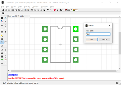
To avoid confusion when combining the package and device, we’re going to name the pads. Eagle still has the vestiges of an old DOS program, and a lot of the commands are accessed by typing a command into the box right above the editor. Type ‘name’ into that box, and click on a pin. We’re going to name each individual pin according to how they’re usually numbered.
With that, save your library, and click on the ‘symbol’ button to create a schematic symbol for this chip. Name the new symbol ATtiny85.
Making a symbol

The symbol is what you will place on your schematic. It defines the electrical connections of the part in your schematic, but unlike the package, it is an abstraction. You could place pins anywhere. In fact, it’s a good idea to lay out your package so it will be easier to draw the schematic.
Just like designing the package, we really only need two buttons on the left-hand toolbar. We use the ‘line’ command to draw a box, and the ‘pin’ button to place pins. These pins are what we use in the schematic to connect parts together. Draw a box and place eight pins around the perimeter, two on one side, and six on the other (it’s common in microcontroller symbols to place power on the left and GPIO on the right like this).

The pin naming convention of the ATtiny85, taken from the Atmel datasheet.
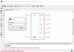
When that’s done, type ‘name’ into the command box, and start labeling your pins. We’re keeping power and ground on one side, so name the top one ‘VCC’ and the bottom ‘GND’. On the other side, label each pin ‘PB0’ to ‘PB4’, making the last pin ‘Reset’.
Save. Now we can combine these two parts into a single package.
Combining the Package and Symbol into a Device

Create a new device, and click the ‘Add’ button in the left-hand toolbar. There’s only one symbol in your library right now, so click that, and drop it on the editor.
Now, we’ll need to select the package this symbol goes with. At the bottom of the window, click the ‘New’ button. Again, there’s only one package in your library, so click it.
Now, we have a window with the symbol in one window, the package in another, and we need to connect the pins in the symbol to the pads in the package. The obvious button to choose is ‘Connect’.

Read the datasheet for the ATtiny85, and make sure all the pins are connected to the correct pads. For the ATtiny85, VCC should be pin 8, Reset should be pin 1, and GND should be pin 4. Connect the rest of the pins to the rest of the pads. When all the pins are connected, hit OK, and save your library.
The ATtiny85 is a small and simple part, but that’s all it takes to create any part in Eagle. To test it out, go to the Eagle Control Panel, create a new schematic, and add a part. Select the library you just created, and place the ATtiny85 device. From the File menu, select ‘Switch to Board’ and you’ll see something like this:

This is not a complete guide to doing everything in Eagle. Even this part of the tutorial did not cover creating labels, text, or anything except the bare minimum of making a part in Eagle. That’s the hardest part of building a PCB in Eagle, and in the next part of this tutorial, we’ll dig into plopping all the parts for our board down on the schematic, nudging them around on the board, and drawing traces between them.
That’s all you need to do to create a single part in Eagle. The next post in this series will go over putting this part in a schematic, creating a board, and sending that file off to a fab. As with all posts in thisCreating A PCB in Everythingseries, we’re looking for suggestions on what to do next. If you have a favorite EDA design tool, leave a note in the comments and we might get around to doing a tutorial for that piece of software.

 My Message
 Suggestions


Enrique Ochoa
2017/2/23 22:41:20
Nice posting! Your sharing is quite in-depth and solves my puzzles all the time. I will keep reading your post.