My Message
 Suggestions


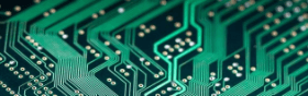
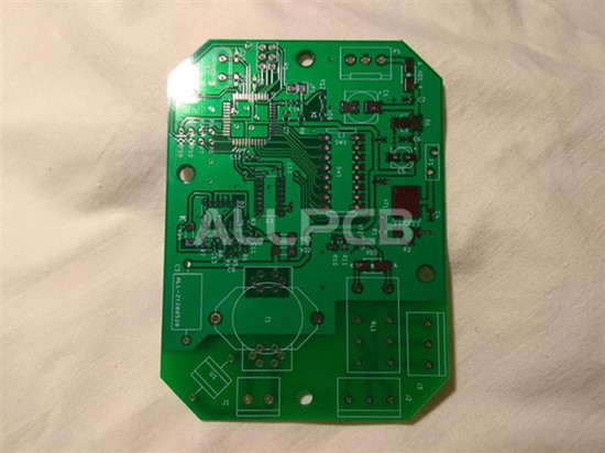
PCB board composition
The current circuit board is mainly composed of the following:
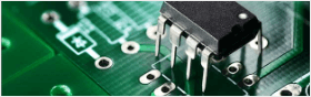
Copper Pattern: The trace is used as a tool for conducting conduction between the originals. In the design, a large copper surface is additionally designed as the grounding and power supply layer. The line and the drawing are made at the same time.
Dielectric: used to maintain the insulation between the circuit and the layers, commonly known as the substrate.
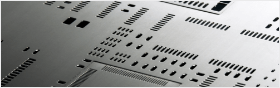
Through hole / via: The via hole can make the two levels above the line conduct each other, the larger via hole is used as the component insert, and the non-via hole (NPTH) is usually used as the surface mount. Positioning and fixing screws for assembly.
Solder resistant /Solder Mask: Not all copper surfaces should be eaten on tin. Therefore, in areas where tin is not eaten, a layer of tin-plated material (usually epoxy) is printed to avoid Short circuit between lines that are not tinned. According to different processes, it is divided into green oil, red oil and blue oil.
Legend /Marking/Silk screen: This is a non-essential structure. The main function is to mark the name and position frame of each part on the circuit board to facilitate post-assembly maintenance and identification.
Surface Finish: Since the copper surface is easily oxidized in the general environment, it is impossible to apply tin (poor solderability), so it will be protected on the copper surface to be tinned. The protection methods include spray coating (HASL), gold (ENIG), silver (Immersion Silver), tin (Immersion Tin), and organic solder resist (OSP). The methods have their own advantages and disadvantages, collectively referred to as surface treatment.
PCB board features
Can be high density. For decades, the high density of printed boards has grown with the integration of integrated circuits and advances in mounting technology.
High reliability. Through a series of inspections, tests and aging tests, the PCB can be reliably operated for a long period of time (usually 20 years).
Designability. For the various performances of PCB (electrical, physical, chemical, mechanical, etc.), the design of printed boards can be realized through design standardization and standardization, with short time and high efficiency.
Productivity. With modern management, it can standardize, scale (quantify), automate and other production, and ensure product quality consistency.
Testability. Established relatively complete test methods, test standards, various test equipment and instruments to detect and identify PCB product qualification and service life.
Assemblyability. PCB products not only facilitate the standardized assembly of various components, but also can be automated, large-scale mass production. At the same time, the PCB and various component assembly components can be assembled to form larger components and systems up to the complete machine.
Maintainability. Since PCB products and various component assembly components are produced in a standardized design and scale, these components are also standardized.
Therefore, once the system fails, it can be replaced quickly, conveniently and flexibly, and the system can be quickly restored. Of course, you can say more about it. Such as miniaturization and weight reduction of the system, high-speed signal transmission, and the like.
Integrated circuit features
The integrated circuit has the advantages of small size, light weight, less lead wires and solder joints, long life, high reliability, good performance, etc., and low cost, and is convenient for mass production. It is widely used not only in industrial and civil electronic equipment such as tape recorders, televisions, computers, etc., but also in military, communication, remote control and other aspects.
The use of integrated circuits to assemble electronic devices has an assembly density that can be increased by several tens to several thousand times compared to transistors, and the stable operating time of the device can be greatly improved.
Integrated circuit application example
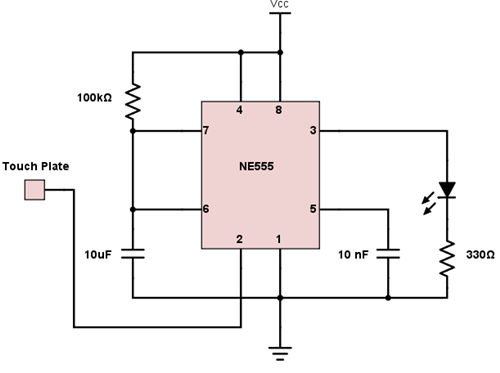
1. 555 touch timer switch
The integrated circuit IC1 is a 555 timing circuit, which is connected here as a monostable circuit. Usually, because there is no induced voltage on the P terminal of the touch panel, the capacitor C1 is discharged through the 7th pin of 555, the output of the 3rd pin is low level, the relay KS is released, and the electric light is not lit.
When it is necessary to turn on the light, touch the metal piece P by hand, and the clutter signal voltage of the human body is added from C2 to the trigger end of 555, so that the output of 555 changes from low to high level, and the relay KS pulls in, the electric light point bright. At the same time, the 555 pin 7 is internally cut off, and the power supply charges C1 through R1. This is the beginning of timing.
When the voltage on the capacitor C1 rises to 2/3 of the power supply voltage, the 555 seventh foot channel causes C1 to discharge, so that the output of the third pin changes from the high level to the low level, the relay is released, the light is extinguished, and the timing ends.
The timing is determined by R1 and C1: T1=1.1R1*C1.
2. single power supply dual power circuit
In the circuit of the drawing, the time base circuit 555 is connected to an unsteady circuit, and the square pin has an output frequency of 20 kHz and a square wave with a duty ratio of 1:1.
When pin 3 is high, C4 is charged; when low, C3 is charged. Due to the existence of VD1 and VD2, C3 and C4 are only charged and not discharged in the circuit. The maximum charging value is EC, and the B terminal is grounded. At both ends of A and C, the dual power supply of +/-EC is obtained. The output current of this circuit exceeds 50mA.

The difference between PCB and integrated circuit
An integrated circuit generally refers to the integration of a chip, such as a north bridge chip on a motherboard. Inside the CPU, it is called an integrated circuit, and the original name is also called an integrated block. The printed circuit refers to the circuit board we usually see, and the solder chip is printed on the circuit board.
The integrated circuit (IC) is soldered on the PCB; the PCB version is the carrier of the integrated circuit (IC). The PCB board is a printed circuit board (PCB). Printed circuit boards appear in almost every electronic device.
If there are electronic parts in a certain device, the printed circuit boards are mounted on PCBs of various sizes. In addition to fixing various small parts, the main function of the printed circuit board is to make electrical interconnections between the various parts above.
Simply put, an integrated circuit integrates a general-purpose circuit into a single chip. It is a whole. Once it is damaged inside, the chip is damaged. The PCB can solder components themselves. If it is broken, the components can be replaced.