My Message
 Suggestions


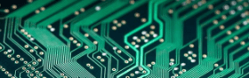
At present, PCB products are moving from traditional to higher density HDI/BUM boards, IC package base boards, embedded component boards and rigid-flex boards. PCBs will eventually go to "printed circuit boards". The limit, in the end, will inevitably lead to the "quality change" from the "electrical transmission signal" to the "optical transmission signal", replacing the printed circuit board with the printed optical circuit board.
Due to the miniaturization, high performance, multi-function of electronic products and the rapid development of high-frequency (speed) signal transmission, PCBs must be rapidly moved from the traditional PCB industry to products characterized by high density and refinement. development of. PCB products have begun, partially or fully integrated into high-density interconnect laminate (HDI/BUM) boards, package-based (loaded) boards, integrated (embedded) component printed boards (ICPCB), and rigid-flexible printing Board (G-FPCB).
In the future, these four PCB type products will become the four bright spots in the PCB industry, and the more advanced printed optical circuit boards with "light signal" transmission and calculation will replace the current "electric signals". Transmission and calculation of printed circuit boards.
HDI/BUM board core board production value accounted for 95%.HDI/BUM boards are PCBs with higher density than conventional printed boards. They can be divided into HDI/BUM boards with “core board” and “core board”.

A "core board" HDI/BUM board is a PCB formed by a higher density of interconnected "layers" on one or both sides of a "conventional printed board". In fact, cored HDI/BUM boards are a form of "conventional printed board" "transition" to higher density PCBs to meet the requirements of very high density installations. At the same time, regardless of equipment, process technology and management, it can better adapt to the best way for the original PCB industry to transition to very high-density PCB products.
If it can be developed and produced on the basis of existing PCB production equipment, testing and technology, it can be developed and produced with low investment, low cost, good continuity and expansion in management and production, and thus is greatly Most PCB manufacturers accept, so the HDI/BUM board with core board accounts for about 95% of the current HDI/BUM board production value.
The HDI/BUM board with core board is significantly more prominent in its high density, such as the 4+12+4 200×300cm2 HDI/BUM board compared to the 400×450 cm2 46-layer buried/blind hole high-rise. The board has higher capacity, better electrical performance and reliability and longevity.
At present, most of the HDI/BUM boards without "core board" are made of conductive adhesive technology, and their use range is limited, so the proportion is small.

IC package substrate solves the most important problem of CTE matching.
The IC package substrate has been developed by "deepening (high density)" based on the HDI/BUM board, or the IC package substrate is a higher density HDI/BUM board. In essence, the primary problem with IC package substrates is the problem of matching (compatibility) with the CTE (thermal expansion coefficient) of the package elements to be packaged, followed by the problem of high density.
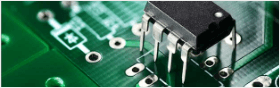
In essence, the PCB provides interconnect and mechanical (physical) support for the components. In today's electronic packaging market, there are three main types of packages: (1) organic substrate packaging; (2) ceramic substrate packaging; (3) ideal size and speed (ie chip level) packaging, such as crystal Wafer Level Package (WLP, Wafer Level Package), Direct Die Attach (DDA). It is clear that conventional PCBs do not have the capability of these advanced packages (low CTE applications), so the PCB industry must develop technologies and products that enable these advanced package substrate materials.
CTE matching (compatibility) issues between package substrate and package element (group). When the CTEs of the two do not match or vary greatly, the internal stress generated after soldering and packaging threatens the reliability and life of the electronic products. Therefore, the CTE matching (compatibility) problem between the package substrate and the packaged component (component) is requiring that the CTE difference between the two is becoming smaller as the mounting density is increased and the solder joint area is reduced.
The IC package substrate is mainly embodied in: The CTE of the substrate material is smaller or matched, that is, the CTE of such an IC substrate is significantly reduced, and the CTE of the chip pin is close (compatible) to ensure reliability; For the package of bare chip (KGD), it is required to increase the density of the IC substrate.
The thickness of the package substrate is thin and the size is small, most of which is less than 70mm×70mm. Most of the thin-type low CTE substrates are used, such as PI material, ultra-thin fiberglass cloth and carbon fiber CCL material.
Integrated Component PCB Embedded in Active Passive Components is the Way Out.
With the development of high-density electronic products, high-frequency signal transmission and high-speed digitalization, the increase in the number of I/O chips and the rapid increase in the number of passive components have increasingly affected the reliability and transmission of electronic products. Signal integrity, the way out is toward integrated (embedded) component printed boards.
Development steps: integration (embedded) passive components (mainly capacitors, resistors and inductors) - → integrated (embedded) active components (IC components).
1. Buried Passive Components
The number of passive components has increased rapidly. The number of passive components will increase rapidly with the increase in IC component integration (or I/O count), high-frequency signal transmission, and high-speed digitization (assembled active/passive components are 1:10—→ 1:20—→1:30—→1:50).
Passive components occupy more and more board area (30%→40%→50%→70%), affecting high density; soldering points of passive components It is also increasing, affecting the reliability of the connection, because the solder joint is one of the main faults of electronic products. The ratio of various element (group) pieces of conventional assembly is shown in the table.
The increase in passive components is bound to cause problems. The increase of passive components has led to more and more solder joints, and the welding reliability is getting lower and lower. The solder joints have always been the biggest failure rate of electronic products; the electromagnetic interference generated by the loop formed by passive components is becoming more and more serious.
The increase in source components increases the board size (area) and the like, which adversely affects high frequency and high speed digital transmission performance.
The use of buried passive components eliminates these effects and significantly improves the integrity and reliability of the transmitted signal.
The buried passive components can be divided into: embedded a single passive component; buried "integrated" (combined capacitors, resistors, etc.) passive components.
2. Buried Embedded Components.
While embedding passive components, embedded embedded components (various IC components) are in the process of development and trial use, and are the road to future development.
The growth rate of rigid-flexible printed boards will accelerate in the future
In 2006, the output value of flexible (including rigid-flexible) printed boards accounted for 17% of the total output value of PCBs. In the future, there will be a faster increase. By 2010, it is expected to reach 25%-30%.
The structure of the rigid-flexible printed board can be varied. The following figure shows the typical two-generation products.
The advantages of rigid-flexible printed boards are many, but the most important ones are: improving reliability in high-density connections (replacement of mechanical connectors, etc.); facilitating miniaturization; installation flexibility (bending or folding) and implementation Three-dimensional (3D) assembly; simplified installation process and maintenance; convenient post-processing, etc., all have obvious advantages. Therefore, it will develop with the development of miniaturization, high performance, and multi-functionality of electronic products.