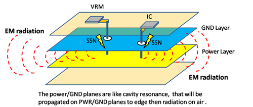
FPGAs can cause severe damage to signals in the system (or other FPGA signals) due to too much high-speed SSO, as this can result in noise called simultaneous switching noise (SSN). SSN is also called ground bounce or VCC bounce. For single-ended standards, SSN is a process that provides transient currents from low to high and absorbs transient currents from high to low, simultaneously switching and causing multiple output drivers. Caused by changes in device voltage and system voltage.

When the high-to-low transition causes the ground to bounce, the low-to-high transition also causes the VCC to drop. Since the capacitor is typically placed between the VCC and the ground plane, the SSN typically exists in these two places. A rebound from low to high is also likely to occur. Thus, the SSO becomes an interfering signal that produces noise that may be coupled to adjacent signals. Too much SSO for a certain area may cause power disturbances.
SSO has become a problem that must be taken seriously for the following two reasons:
1. The switching time has dropped drastically;
2. The reduction in via size and trace width plus larger board thickness has pushed the board inductance.
This will greatly increase the likelihood of a rebound in the field. Larger load capacitance can also cause SSN, albeit to a lesser extent. When the effective VCC is lower than the expected value, resulting in a lower conversion speed of the I/O buffer than the expected speed, the SSN may also cause timing problems to become prominent.
There are several ways to reduce the SSN. Some devices simplify this problem by simply limiting the choice of I/O standards, but not all devices can do so. Some vendors recommend distributing the high-speed bus output to the entire die. If SSN is your only concern, then this is definitely a good suggestion. However, if you follow this advice, there are 2 basic questions that will come out.
First, this can lead to downstream connectivity issues, as spreading signals across the entire die often leads to more trace crossings. This leads to the need for more signal wiring layers. Second, most designs require careful study before spreading the signal, because block/interval compatibility issues can arise when a bus is spread outside a particular block or region. Therefore, if you can carefully spread a smaller bus into one or two blocks/areas while considering connectivity, the system will work fine.
If you are bothered by a design with adjacent high-speed switching outputs, there are several techniques that can help you solve potential SSN problems. First make proper layout and decoupling of your design. For decoupling, use power and ground plane pairs as close as possible, separated by an SMT capacitor. Decoupling with SMT capacitors also helps to reduce inductance, which is a major factor in generating system noise.
If you still feel the need to use decoupling capacitors (to reduce the SSN), you should position these capacitors as close as possible to the high speed output pins. A study by Altera found that if these capacitors are more than 1 inch from the pin, these capacitors become extremely inefficient when decoupled with the appropriate SMT capacitors.

Other suggestions for reducing SSN or its possible effects include: avoiding sensitive signals (reset, clock, and enable, etc.) near SSO; if possible, using smaller offset outputs and using the lowest inductance vias; A suitable position insertion delay causes the output signals to alternate. Even if PCB production has been completed, this recommendation can still be applied.
Refer to the relevant material that will be connected to the device on the FPGA. For each device, determine the maximum input low voltage threshold (in millivolts). This is the maximum voltage required by the FPGA to drive the device, so the device can still detect an active logic low state (maximum VIL value). Also, determine the maximum input negative pulse signal (in millivolts) that the device can tolerate and continue to operate.

In some cases, the maximum allowable ground bounce may not be or is not just the value given above. Instead, the maximum system ground bounce is determined by obtaining the minimum of the maximum input low voltage threshold, the maximum input negative pulse signal, or the maximum bounce of all devices.
Similar FPGA buses are then grouped according to the number and type of network connections with similar load characteristics. Next, study the number of power and ground pins for each section, region, or block, and the number of SSOs allowed for each power and ground pin pair for each I/O standard used. These numbers can be used to calculate the total capacitive load of each group and the capacitance of each output drive to determine the maximum SSO that can be tolerated.
You should also consult with the supplier to determine if you exceed the recommended number of SSOs based on each block and each pair of blocks, provided that the vendor has studied these issues. At the same time, because there are multiple factors that can cause SSN, it is best to build a robust system with built-in anti-noise performance. Otherwise, use a device that limits the I/O standard for each pin, which reduces the potential SSN problem.
In FPGA design, you may find that there is most controversy about the processing of differential signals. Similar to SSN, it's best to get as much information as possible from vendors, books, and user groups. Also, consult your layout department to find out what recommendations they recommend and information before deciding on a plan.
The main argument begins with whether the differential signal pair should use wide-edge coupling or edge coupling, and how much coupling should exist between each pair. The answer is usually “determined on a case-by-case basis”, so specific research is needed.
If you are not sure why you need to choose a differential I/O standard for a single-ended signal, the answer is simple. With differential signals, you can almost completely control the loop of the signal. Because this is part of the signal pair, and theoretically no current from the signal pair should occur on any ground (or power) plane.
It is assumed here that the pair of traces have equal lengths, are arranged in adjacent regions and have a constant pitch, and the trace impedance is constant and matched. In addition, with single-end sign, it is difficult to control the signal back haul, and testing the return of a signal can be futile.
The main bad points for the differential signals is that they demands two traces to be close to each other. This can be a big challenge when distributing hundreds of signals on a single PCB.

 My Message
 Suggestions


