My Message
 Suggestions


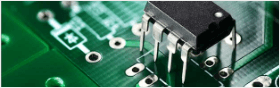
The product I'm running currently consist a mix of 20 mil pitch QFP, 50 mil pitch, 0402, BGA and variable size of connectors from small to big, on OSP finished PCB. Running intrusive reflow with a mix packages is a real headache, especially when you have to hv step up at certain location, where the clearance to the neighboring component ( 0402) is very limited. If I were to have a good DFM, what is the best clearance for the step up i.e. 12 mil from 6 mil thickness. FYI, the metal squeegee is purposely cut, to ensure flexibility at printing.
2ndly, taking into consideration that the good solder wetting of OSP coated boards occurs only where the flux comes into contact with the pads, I've modified the stencil opening for fine pitch i.e maintaining the length 1:1 and reduce the width by 2 - 4 mil from the pad size ( to prevent shorts). This is done with the intention of preventing the reflowed board from having an exposed copper ( small portion at the end/edge of the copper pad )but I failed to eliminate the pad with an exposed copper. Why is this happening and how should I overcome this problem. FYI, the experiment was also done with stncil aperture which purposely design longer than the pad length but still we tends to see a small portion of the pad at the edge end, exposed.
I've explaind to the our customer about the OSP finised characteristic but they asked me why..and I kind of "doinkk?" To be honest, I'm not happy with this "exposed copper" things, taking into consideration about the capillary action over the time.
I plan to go back to HASL, what do you guys think? Coplanarity issue should be minimal with 20 mil and above, rite ? Rather than touching-up every single point on the board, and induce other problem to the board.