My Message
 Suggestions


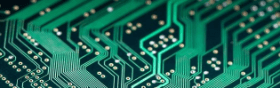
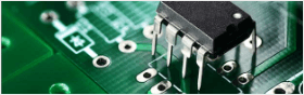
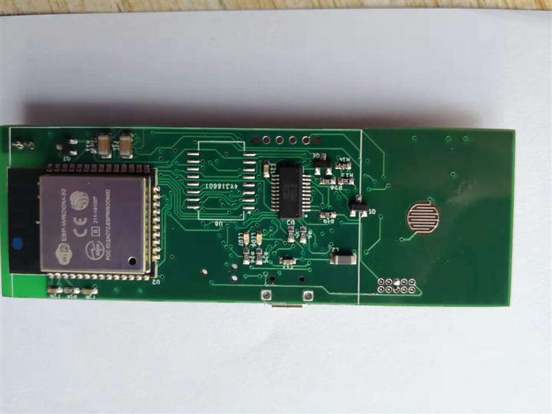
Chip-on-board (COB), semiconductor chip is placed on the printed circuit board, and the electrical connection between the chip and the substrate is achieved by wire stitching. The electrical connection between the chip and the substrate is achieved by wire stitching and covered with resin to ensure reliability. Although COB is the simplest bare chip placement technology, its packaging density is far less than that of TAB and flip chip bonding.
The chip on board (ChipOnBoard, COB) process first covers the wafer placement point with a thermally conductive epoxy resin (usually an epoxy resin doped with silver particles) on the surface of the substrate, and then directly places the silicon wafer on the surface of the substrate and heats it to silicon. The sheet is firmly fixed to the substrate, and then an electrical connection is directly established between the silicon wafer and the substrate by wire bonding.
Compared with other packaging technologies, COB technology is cheap (only about 1/3 of the same chip), space saving, and mature technology. However, any new technology can't be perfect when it first appears. COB technology also has the disadvantages of needing another welding machine and packaging machine, sometimes the speed can not keep up, and the PCB patch is more strict and maintenance-free.
Some chip-on-board (CoB) layouts can improve IC signal performance because they remove most or all of the package, which removes most or all of the parasitic devices. However, with these technologies, there may be some performance issues. In all of these designs, the substrate may not be well connected to VCC or ground due to the leadframe sheet or BGA mark. Possible problems include thermal expansion coefficient (CTE) problems and poor substrate connections.
The Main Welding Method of COB:
(1) Thermocompression Bonding
The wire is pressed and welded together by heating and pressing. The principle is that the heating zone and the pressing force cause the weld zone (such as AI) to plastically deform and destroy the oxide layer on the pressure welding interface, thereby making the attraction between the atoms reach the purpose of "bonding". In addition, the two metal interfaces are not When the flat heating and pressurization, the upper and lower metals can be inlaid with each other. This technique is generally used as a chip on board glass COG.
(2) Ultrasonic welding
Ultrasonic welding uses the energy generated by the ultrasonic generator. Through the transducer's magnetic field induction of ultra-high frequency, it rapidly expands and contracts to produce elastic vibration, which causes the file to vibrate accordingly, and at the same time exerts a certain pressure on the file, so the file is Under the joint action of these two forces, the AI wire is rapidly rubbed on the surface of the metallized layer such as (AI film) of the welded zone, and the surface of the AI wire and the AI film is plastically deformed. This deformation also destroys the interface of the AI layer. The oxide layer is such that the two pure metal surfaces are in intimate contact to achieve atomic bonding, thereby forming a weld. The main welding material is aluminum wire welding head, which is generally wedge-shaped.
(3) Gold wire welding
Ball bonding is the most representative soldering technique in wire bonding, because the current semiconductor package diodes and triode packages are all AU ball bonded. Moreover, it is easy to operate, flexible, and has a firm solder joint (the AU wire with a diameter of 25 UM is generally 0.07 to 0.09 N/dot), and has no directionality, and the welding speed can be as high as 15 points/second or more. Gold wire welding is also called hot (pressure) (super) sonic welding. The main bonding material is gold (AU) wire bonding head is spherical, so it is ball bonding.
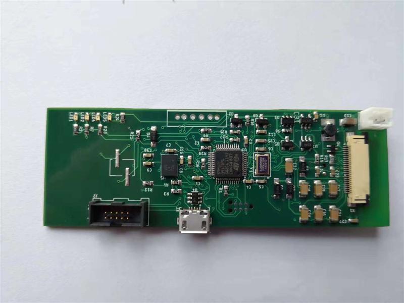
COB Packaging Process
Step 1: crystal expansion. The expansion of the entire LED chip film provided by the manufacturer is uniformly expanded by the expansion machine, so that the LED crystal grains closely attached to the surface of the film are pulled apart to facilitate the puncturing.
Step 2: adhesive. Place the crystal-expanded crystal expansion ring on the surface of the adhesive machine with the silver paste layer and the silver paste on the back.
Point silver paste. Suitable for bulk LED chips. Use a dispenser to spot the right amount of silver paste on the PCB printed circuit board.
Step 3: inserting the crystal-filled ring of the silver paste into the thorn frame, and the operator punches the LED chip on the PCB printed circuit board with a lancet under the microscope.
Step 4: put the punctured PCB printed circuit board into a heat cycle oven for a period of time, and wait for the silver paste to solidify (not permanently set, otherwise the LED chip coating will be baked yellow, that is, oxidized, to bond Cause difficulties). If there is LED chip bonding, the above steps are required; if only the IC chip is bonded, the above steps are cancelled.
Step 5: Stick the chip. Use a dispenser to apply a proper amount of red glue (or vinyl) to the IC position of the PCB printed circuit board, and then use an antistatic device (vacuum pen or sub) to properly place the IC die on the red or black glue.
Step 6: Drying. The bonded die is placed in a thermal cycle oven and placed on a large flat heating plate for a period of time, or it can be naturally cured (longer time).
Step 7: Bonding (line). The wafer (LED die or IC chip) is bridged with the corresponding pad aluminum wire on the PCB by an aluminum wire bonding machine, that is, the inner lead of the COB is soldered.
Step 8: pretest. Use a special inspection tool (the COB has different equipment for different purposes, the simple one is a high-precision regulated power supply) to detect the COB board and rework the unqualified board.
Step 9: Dispensing. The dispenser is equipped with a suitable amount of AB glue to the bonding LED die. The IC is packaged in black plastic and then packaged according to customer requirements.
Step 10: Curing. The sealed PCB printed circuit board is placed in a heat cycle oven to be kept at a constant temperature, and different drying times can be set according to requirements.
The eleventh step: post-test. The packaged PCB printed circuit board is then tested for electrical performance using a dedicated inspection tool to distinguish between good and bad.