My Message
 Suggestions


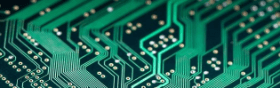
The manufacturing process of the PCB begins with a "substrate" made of glass epoxy (Glass Epoxy) or made of base with something similar material.
The first step in the production is to create wiring that connects the parts. We use a subtractive transfer method to present the working film on a metal conductor. The way is to lay a thin layer of copper on the entire surface and remove the excess. Additive Pattern Transfer is another way to use less people. This is a way to apply copper wire only where it is needed, but we won't talk much about it here.
If you are making a double-panel, the PCB will be coated with copper foil on both sides. If you are making a multi-layer board, the next step will stick the boards together.
The next flow chart shows how the wire is soldered to the substrate.
Positive photo resist is made of sensitizer, which dissolves under illumination (negative photo resist is decomposed if not illuminated). There are many ways to handle photo resist on copper surfaces, but the most common way is to heat it and roll it on a surface containing a photo resist (called a dry film photo resist). It can also be sprayed on the head in a liquid state, but the dry film type provides a higher resolution and can also make a thinner wire.
The hood is just a template for the PCB layer in the manufacturing process. Before the photo resist on the PCB is exposed to UV light, the hood overlying it prevents some areas of the photo resist from being exposed (assuming a positive photo resist). These places covered by photo resist will become wiring.
Other bare copper portions to be etched after development of the photo resist. The etching process can immerse the board in an etching solvent or spray the solvent onto the board. Commonly used as an etching solvent are ferric chloride (Ferric Chloride), alkaline ammonia (Alkaline Ammonia), sulfuric acid plus hydrogen peroxide (Sulfuric Acid + Hydrogen Peroxide), and copper chloride (Cupric Chloride). The remaining photo resist is removed after the etching is completed. This is called a stripping process.
Drilling and plating
If you are making a multi-layer PCB board and have buried or blind holes in it, each layer must be drilled and plated before bonding. If you don't go through this step,

there is no way to connect to each other.
After drilling the machine equipment according to the drilling requirements, the hole must be plated (Plated-Through-Hole technology, PTH). After metal treatment inside the hole, the internal layers can be connected to each other. Before starting the plating, the debris in the hole must be removed. This is because the resin epoxide will undergo some chemical changes after heating, and it will cover the inner PCB layer, so it must be removed first. Both the removal and plating operations are done in a chemical process.
Multilayer PCB press
Each monolithic layer must be laminated to produce a multilayer board. The pressing action includes adding an insulating layer between the layers, and sticking each other. If there are several layers of vias, then each layer must be processed repeatedly. The wiring on the outer sides of the multilayer board is usually processed after the multilayer board is pressed.
Treatment of solder mask, screen printing surface and gold finger plating
Next, the solder resist is overlaid on the outermost wiring so that the wiring does not touch the plating part. The screen printing surface is printed on it to indicate the position of each part. It cannot cover any wiring or gold fingers, otherwise it may reduce the solderability or the stability of the current connection. The gold finger portion is usually plated with gold so that a high quality current connection is ensured when inserted into the expansion slot.
Test the PCB for shorts or open circuits and test it optically or electronically. Optical scanning is used to find defects in each layer, and electronic testing is usually done with a flying probe (Flying-Probe) to check all connections. Electronic tests are more accurate in finding short circuits or open circuits, but optical tests can more easily detect problems with incorrect gaps between conductors.

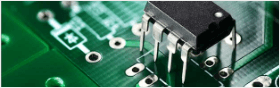
Parts installation and welding
The last step is to install and solder the parts. Both THT and SMT parts are machined to be placed on the PCB.
THT parts are usually soldered in a way called Wave Soldering. This allows all parts to be soldered to the PCB at a time. First cut the pin close to the board and bend it slightly to allow the part to be fixed. The PCB is then moved to a water wave of the co-solvent and the bottom is contacted with a co-solvent so that the oxide on the bottom metal can be removed. After heating the PCB, this time it is moved to the molten solder, and the soldering is completed after contact with the bottom.
The way to automatically weld SMT parts is called Over Reflow Soldering. The paste solder containing the solvent and the solder is processed once after the parts are mounted on the PCB, and then processed after being heated by the PCB. After the PCB is cooled, the soldering is completed, and the next step is to prepare for the final test of the PCB.