My Message
 Suggestions


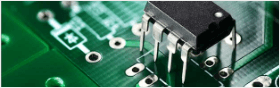
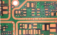
Via holes paly the role of interconnected conduction. The development of the electronics industry promotes the development of PCB, putting forward higher requirements on PCB production process and surface mount technology. The plug hole process appears and meets the following requirements:
(A) the inner hole can be copper; solder can be plug can not plug;
(B) must have tin lead lead, there is a certain thickness requirements (4 microns) and shall not have solder resist ink into the hole, resulting in tin beads in the hole;
(C) vias must have solder mask ink plug hole, not light, no tin ring,and have tin beads and leveling requirements.
There are five main roles of plug hole:
(A) to prevent PCB a short circuit caused by tin from the through-hole to the element surface in wave soldering; especially when we put the vias on the BGA pad, you must first do plug hole, and then gold-plated for easy BGA welding.
(B) to avoid the flux residue in the vias;
(C) after electronic plant surface mount and component assembly, the PCB will be only finished in the test machine to form a negative pressure in vacuum
(D) to prevent the surface of the solder paste into the hole, affecting the placement;
(5) to prevent the wave soldering tin beads when the pop-up, resulting in short circuit.