 My Message
 Suggestions


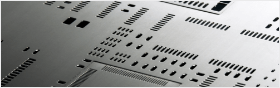
To design a flex PCB is slightly different from rigid
PCBs. Compared with rigid PCBs, flex PCBs can provide major savings in
manufacturing cost and reduce space consumption. And a well-designed flex PCB
is durable, lightweight and easy to install and so on. Thus, flex PCB design
must be optimized for its material and usage.
There are various methods to ensure a high-quality flex PCB design. Here are six must-knows for you should pay attention to in your first flex PCB design:
1. Do not place circuit traces too close to opening
When circuit traces are close to the edge, shortages may happen. For cover-lay, the trace to mask opening can be as close as 3 mils. As for soldermask, 3 mils will lead to misregistration or undercut issues. A distance of at least 4 mils for soldermask is highly recommended in flex PCB design.
2. Understand your flex PCB materials
Flex PCB materials have less dimensional stability than rigid PCBs so that they usually require looser outline tolerance than other boards. You may resort to a hard tool or laser cutting that is expensive when depending on profile tolerance.
On the other hand, flex PCB materials may contain acrylic
adhesives. It is important to make the pads as big as possible because those
chemicals will become soft when heated. Spurs, anchors and teardrops can be
helpful to stabilize the outer layer and reduce stress.
3. The bendability of flex PCB
How many times flex PCB will be bending and what it can
bend are important in design. The times it can bend directly decide whether the
PCB is a static or dynamic board. A static board is considered bend -to-
install, with less than 100 times bending in its lifetime. On the other hand, a
dynamic board should be designed more robust in nature and is capable of tens
and thousands of flexing. Bend radius, the min amount of bendiness for flex
area, must be indentified properly in PCB design, which allows for the
necessary bends without damaging the copper.
4. Reduce risks in flex vias
Vias are able to crack or break flex PCB designs if vias are not teardropped or anchors are not contained. Besides, annular rings should be as large as possible to reduce the risk in flex vias.
5. Pay attention to flex trace routing
Circuitry layout is important for a PCB. A larger radius is preferable here to the sharp angles that shorten a board’s lifespan. Moreover, you’d better to avoid I-beaming, minimizing the stress and thinning out copper circuit. And curved traces cause lower stress than angle ones. Also, traces should be kept perpendicular to the overall bend and staggered on the top and bottom if placed on a flex PCB with more than two layers.
6. Remember to place flex layers in the center when stackup
For rigid-flex PCBs, placing flex layers in the center of stackup protects outer layer plating from exposure, which also simplifies manufacture and enhances impedance control in the flex area.


el.mehdi.fakir
2017/2/15 18:39:19
Truly enjyed reading your posts.