My Message
 Suggestions


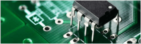
Common Defects and Solutions in the Dispensing Process
Drawing/tailing
Drawing/tailing is a common defect in dispensing. The causes are usually too small, the dispensing pressure is too high, the distance between the plastic nozzle and the PCB is too large, the adhesive is out of date or the quality is not good, and the adhesive is applied. The viscosity is too good, it can't be restored to room temperature after taking out from the refrigerator, and the amount of dispensing is too large.
Solution: Change the nozzle with larger inner diameter; reduce the dispensing pressure; adjust the "stop" height; change the glue, select the rubber of suitable viscosity; the patch glue should be restored to room temperature after being taken out of the refrigerator (about 4h) Put into production; adjust the amount of glue.
Plastic Nozzle Blocked.
The fault phenomenon is that the glue nozzle has less glue or no glue point. The cause is generally that the pinhole is not completely cleaned; the paste glue is mixed with impurities, and there is plugging phenomenon; the incompatible glue is mixed.
Solution: Change the clean needle; change the quality of the patch glue; the patch rubber grade should not be mistaken.
Empty Play
The phenomenon is that only the dispensing action, but no glue amount. The reason is that the patch glue is mixed into the bubble; the nozzle is blocked.
Solution: The glue in the syringe should be deaerated (especially the glue installed by itself); replace the nozzle.
Component Shift
The phenomenon is that the component is displaced after the patch adhesive is cured. In serious cases, the component pins are not on the pad. The reason is that the glue of the patch glue is not uniform, for example, the chip component has more than one glue in the two points; When the component is displaced or the initial adhesive force of the patch glue is low; the PCB is placed for too long after dispensing, and the glue is semi-cured.
Solution: Check if the nozzle is clogged, remove the uneven rubber; adjust the working condition of the placement machine; change the glue; the PCB placement time after dispensing should not be too long (less than 4h)
Wave Soldering will Fall off
The phenomenon is that the bonding strength of the components after curing is not enough, lower than the specified value, sometimes the film will appear to fall off. The reason is because the curing process parameters are not in place, especially the temperature is not enough, the component size is too large, and the heat absorption is large; The curing light is aging; the amount of glue is not enough; the component/PCB is polluted.
Solution: Adjust the curing curve, especially to improve the curing temperature. Usually, the peak curing temperature of the heat curing adhesive is about 150 °C. If the peak temperature is not reached, it will cause the film to fall off. For the light curing glue, it should be observed whether the curing light is aging. Whether the lamp is black or not; the amount of glue and the contamination of the component/PCB are all issues that should be considered.
Component Pin Floating/Shifting after Curing
The phenomenon of this failure is that the component leads float or shift after curing. After the wave soldering, the tin material will enter the pad. In severe cases, short circuit and open circuit will occur. The main reason is uneven patch adhesive and patch adhesive amount. Excessive or patch component offset.
Solution: Adjust the dispensing process parameters; control the amount of dispensing; adjust the processing parameters of the patch.

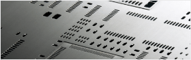
Solder Paste Printing and Patch Quality Analysis
The quality problems caused by poor solder paste printing are as follows:
1. Insufficient solder paste (partial lack or even lack of overall) will lead to insufficient solder joints, component open circuit, component offset, and component erection.
2. Solder paste adhesion will lead to short circuit and component misalignment after soldering.
3. The overall deviation of solder paste printing will lead to poor soldering of the whole board components, such as less tin, open circuit, offset, vertical parts, etc.
4. Solder paste tip is easy to cause short circuit after soldering.
The Main Factors Leading to Insufficient Solder Paste:
1. When the printing press is working, the solder paste is not added in time.
2. The quality of the solder paste is abnormal, and there are foreign materials such as hard blocks.
3. The solder paste that has not been used up before has expired and is used twice.
4. Board quality problems, there are inconspicuous covers on the pads, such as solder resist (green oil) printed on the pads.
5. The fixed clamping of the board in the printing press is loose.
6. The solder paste is missing and the stencil is uneven.
7. Solder paste is missing on the stencil or circuit board (such as PCB packaging, stencil wiping paper, foreign matter floating in the ambient air, etc.).
8. The solder paste scraper is damaged and the stencil is damaged.
9. The equipment parameters such as pressure, angle, speed and demoulding speed of the solder paste scraper are not suitable.
10. After the solder paste is printed, it is accidentally knocked out due to human factors.

The Main Factors Leading to Solder Paste Adhesion:
1. Circuit board design defects, the pad pitch is too small.
2. Stencil problem, the pupil position is not correct.
3. The stencil is not wiped clean.
4. The problem of the stencil makes the solder paste fall off badly.
5. Solder paste performance is poor, viscosity, collapse is unqualified.
6. The fixed clamping of the board in the printing press is loose.
7. The equipment parameters such as pressure, angle, speed and demoulding speed of the solder paste scraper are not suitable.
8. After the solder paste is printed, it is squeezed and stuck due to human factors.
The Main Factors Leading to the Overall Deviation of Solder Paste Printing.
1. The positioning reference point on the board is not clear.
2. The positioning reference point on the board is not aligned with the reference point of the stencil.
3. The fixed clamping of the circuit board in the printing machine is loose. The positioning thimble is not in place.
4. The optical positioning system of the printing press is faulty.
5. Solder paste missing printed stencil opening does not match the design file of the circuit board.
The Main Factors that Lead to the Printing of Solder Paste Tip:
1. There are problems with the performance parameters such as solder paste viscosity.
2. There is a problem with the setting of the demolding parameters when the circuit board is separated from the missing printed board.
3. There is a burr on the hole wall of the stencil of the stencil.