My Message
 Suggestions


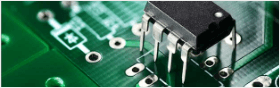
An Introduction to the Solder Mask Layer
The solder mask layer, which refers to the part of the board to be covered with green oil (solder resist ink). It will cover the solder mask oil except pads; this can avoid putting TIN in those places. Apply a layer of paint to each part of the pad to protect the pad from being painted. In Gerber files, its suffix usually be like: .GTS/.GBS.
In Gerber files, the solder mask is a negative output, so finally the solder mask is matched to the exposure copper or bare PCB, Not the part of covering solder mask oil. Sometimes, in order to increase the thickness of the copper, it is designed in the solder mask layer and then let the copper/tracks being exposed, and after surface treatment, these parts will be added thickness by HASL/ENIG.

The Requirements for Solder Mask Layer
Process requirements:
The role of the solder-mask is very important in controlling soldering defects during the reflow soldering process, and the PCB designers should minimize the spacing or air gap around the pad features. While many PCB engineers prefer to separate pad features by solder mask on the board. It will require special consideration for the pin spacing and pad size of the fine pitch components.
Although it is acceptable to not make pad discrimination on the four sides of the QFP, it may be more difficult to control the tin bridge between the component pins. For BGA solder masks, many companies offer a solder mask that does not touch the pads but covers any features between the pads to prevent tin bridges. That is called solder mask - bridge.
Most surface mount PCBs are covered with a solder mask, but the solder mask coating, if it is thicker than 0.04 mm ("), it may affect the application of solder paste. For the surface mount PCBs, especially those for that fine pitch components; it can be required with a low profile photosensitive solder mask.
Production Process:
The solder mask material must be used by a liquid wet process or a dry film laminate. The dry film solder resist is supplied in a thickness of 0.07-0.1mm (0.03-0.04") and it is suitable for some surface mount products, but this material is not recommended for close pitch applications.
A few companies offer thin enough to meet Dry-pitch standard dry film, but many companies can provide liquid photo resist. And in typically, the solder mask opening should be 0.15 mm (0.006") larger than the pad. This allows a gap of 0.07 mm (0.003") on all sides of the pad. The Low profile liquid photo solder mask materials are economical and they are typically specified for surface mount applications, which can provide more precise feature size and clearance.
An Introduction to the Soldering Paste Layer
For the soldering paste layer, it is used when the machine is patched and which corresponding to the pad of the chip component. In SMT processing, it will make a stencil that is a steel plate is used to punch the hole on the PCB corresponding to the component pad, and then the solder paste is applied on the steel plate. When the PCB is under the steel plate, the solder paste is used and leaking down, then just solder paste can be applied to each pad. Then usually the solder paste layer could not be larger than the actual pad size. It is most appropriate "<=" be used.
In Gerber files, its suffix usually be like: .GTP/.GBP.

Solder Paste: It is a fluxing material that provides better soldering. Make electronic parts better with bare exposed surfaces pads.The required dimensions and surface-mount components are almost identical and require the following main elements:
1. BeginLayer: ThermalRelief and AnTIPad are 0.5mm larger than the actual size of the regular pad.
2. EndLayer: ThermalRelief and AnTIPad are 0.5mm larger than the actual size of the regular pad.
3. DEFAULTINTERNAL: the middle layer.

Solder Mask and Solder Paste Layer
The solder mask is mainly used to prevent the PCB pads /tracks from being directly exposed to the air and then it can protect well. The soldering paste layer is used to make the stencil for the steel mesh factory, and the steel mesh can accurately place the solder paste on the soldering pad, then it can be soldered when the tin is applied.
PCB Soldering Paste Layer and Solder Mask Layer
Both layers are used for soldering. It not just means to put the tin, or covering green oil, it is like following:
1.The solder mask means to open the window on the whole piece of solder resist green oil, the purpose is to allow welding;
2.By default, the green oil (solder mask oil) should be applied to areas where there is no need soldering;
3. The soldering paste layer is used for the assembly in the SMT process. If the components are DIP, then there is no need soldering paste layer.
In general speaking, the solder mask means to open the window on the whole piece of solder resist green oil, the purpose is to allow welding, all the pads and patches to be inserted into the part; it just be windowed to prevent ink coverage. The solder paste layer refers to the file layer which generated by the .pcb file, and only if the patch has a solder-proof window. By default, the green oil is required in areas where there is no solder mask. The paste mask layer is used for patch packaging.
The solder mask is used by the circuit board manufacturers, and the solder paste layer is used for the steel mesh and the companies printing solder paste to the PCB, which can help to put suitable paste on PCB and finished the components soldering.