My Message
 Suggestions


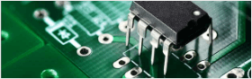
For electronic products, the printed circuit board design is a design process that must be passed from electrical schematic to a specific product. The rationality of its design is closely related to product production and product quality.
For many people who are just engaged in electronic design, there is less experience in this area. Although they have learned the printed circuit board design software, the printed circuit boards are often designed with many problems, but in many electronic publications, there are few articles in this regard. The author of this article has been engaged in the design of printed circuit boards for many years. Here, I share the experience of printed circuit board design with others, hoping to play a role and help the electrical engineering to avoid such problems during their design process for PCB.

About board layout:
The usual order in which components are placed on a printed circuit board:
Place components in a fixed position that closely match the structure, such as power sockets, indicators, switches, connectors, etc. After these devices are placed, they are locked by the LOCK function of the software so that they will not be accidentally moved later;
Place special components and large components on the line, such as heating components, transformers, ICs, etc.
Place small devices. The distance between the components and the edge of the board: if possible, all components are placed within 3mm from the edge of the board or at least greater than the thickness of the board. This is due to the high-volume production of the plug-in and wave soldering. It need to be used for the mounting rail. And at the same time, in order to prevent the edge portion from being damaged due to the shape processing. If there are too many components on the printed circuit board, if it is necessary to exceed the 3mm range, a 3mm auxiliary edge can be added to the edge of the board, and the auxiliary side is opened V-shaped. The tank can be cut by hand during production.

Isolation between high and low voltage: There are high voltage circuits and low voltage circuits on many printed circuit boards. The components of the high voltage circuit are need separated from the low voltage parts. The isolation distance is related to the withstand voltage. Usually, At 2000kV, the distance between the boards should be 2mm. On this basis, the ratio should be increased. For example, if you want to withstand the 3000V withstand voltage test, the distance between the high and low voltage lines should be more than 3.5mm. In many cases, in order to avoid Crawling, it need to design the slotting between high and low voltage on the printed circuit board.
Printed Circuit Board Traces:
The layout of printed conductors should be as short as possible, especially in high-frequency circuits; and the turns of printed conductors should be rounded, while the right or sharp corners can affect electrical performance in high-frequency circuits and high wiring densities. When two panels are wired, the conductors on both sides should be perpendicular, oblique, or curved, this can avoid parallel to each other to reduce parasitic coupling; the printed conductors used as input and output of the circuit should avoid adjacent parallelism as much as possible. In order to avoid feedback, it is best to add a grounding wire between these wires.
Printed Wire Width:
The width of the wire should be suitable for electrical performance and easy to produce. Its minimum value depends on the current to withstand, but the minimum should not be less than 0.2mm. In high-density, high-precision printed circuits, the wire width and the pitch is generally 0.3mm; the wire width should be considered in the case of high current. The single-panel experiment shows that when the copper foil thickness is 50μm, the wire width is 1~1.5mm, and the current is 2A, the temperature rise is very small. Generally, a wire with a width of 1 to 1.5 mm may be used to meet the design requirements without causing a temperature rise.
The common ground of the printed conductor should be as thick as possible. If possible, it is better use a line larger than 2~3mm. This is especially important in circuits with microprocessors because the local line is too thin due to the current flowing. The ground potential changes, then the level of the microprocessor timing signal is unstable, which will degrade the noise margin; in the DIP package, the IC pin can be applied with the principle of 10-10 and 12-12, that is, when the two feet When passing 2 wires, the pad diameter can be set to 50mil, the line width and the line pitch are 10mil. When only one wire is passed between the two legs, the pad diameter can be set to 64mil, the line width and the line spacing are 12mil. .
Printed conductor spacing:
Adjacent conductor spacing must meet electrical safety requirements, and the spacing should be as wide as possible for ease of operation and production. The minimum spacing must be at least suitable for the voltage to withstand. This voltage typically includes the operating voltage, additional ripple voltage, and other peak voltages. If the relevant technical conditions allow for some degree of metal residue between the wires, the spacing will be reduced. Therefore, the designers should take this factor into consideration when considering voltage. When the wiring density is low, the pitch of the signal lines can be appropriately increased, and the signal lines with high and low levels should be as short as possible and the pitch should be increased.
Shielding and grounding of printed conductors:
The common ground wire of the printed conductor should be placed as far as possible on the edge of the printed circuit board. The copper foil should be kept as much as possible on the printed circuit board, so that the shielding effect is better than that of a long ground wire. The transmission line characteristics and shielding effect will be improved, and the function of reducing the distributed capacitance will be achieved.

The common ground of the printed conductors preferably forms a loop or a mesh because there are many integrated circuits on the same board, especially when there are many power-consuming components, that resulting in a ground potential difference due to pattern limitations. Therefore, the noise margin is lowered, and when the loop is made, the ground potential difference is reduced.
In addition, the grounding and power supply graphics should be parallel to the flow direction of the data as much as possible. This is the secret to suppress the noise enhancement. The multilayer printed circuit board can take several layers as the shielding layer. The power layer and the ground layer can be seen. For the shielding layer, generally the wiring layer and the power supply layer are designed on the inner layer of the multilayer printed wiring board, and the signal lines are designed on the inner layer and the outer layer.