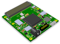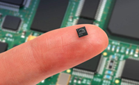
Field-programmable gate arrays (FPGAs) were introduced more than three decades ago, and since then they have evolved, giving way to new generations of FPGAs with better logic density and performance that can be used in a broader range of applications.
The first FPGA was invented by Ross Freeman (cofounder of Xilinx) in 1985 and since then their logic capacity has enhanced greatly and they have become a popular choice because FPGA systems can be reprogrammed after manufacturing to implement the user’s final desired application. Some FPGAs can be reprogrammed infinite times and some limited times.
In general terms, FPGAs are programmable silicon chips with a collection of programmable logic blocks surrounded by Input/Output blocks that are put together through programmable interconnect resources to become any kind of digital circuit or system. FPGAs developed from programmable read-only memory (PROM) and programmable logic devices (PLDs).
Unlike processors, FPGAs are truly parallel in nature. Each independent processing task is assigned to a dedicated section of the chip. Therefore, the performance of one part of the application is not affected when more processing tasks are added.
FPGA Architecture
A precise architecture of an FPGA varies from manufacturer to manufacturer. Here, we present a generic FPGA structure that contains the following elements:
• Programmable logic blocks: Logic blocks can be formed from thousands of transistors to millions of transistors. They implement the logic functions required by the design and consist of logic components such as transistor pairs, look-up tables (LUTs), and Carry and Control Logic (flip flops and multiplexers).
• Programmable I/O blocks: They connect logic blocks with external components via interfacing pins.
• Programmable interconnect resources: They are electrically programmable interconnections (pre-laid vertically and horizontally) that provide the routing path for the programmable logic blocks. Routing paths contain wire segments of varying lengths which can be interconnected via electrically programmable switches. The FPGA density depends of the number of segments in used for routing paths.
Types of FPGAs
The routing architecture affects density and performance of the FPGA. Based on internal arrangement of blocks, FPGAs might be classified into three categories:
• Symmetrical arrays: This arrangement consists of logic blocks arranged in rows and columns of a matrix and interconnect resources between them. This symmetrical matrix is surrounded by I/O blocks that connect it to the outside world (Fig.1).

1. Symmetrical arrays consist of a two-dimensional array of logic modules interconnected by vertical and horizontal programmable interconnect resources. (Courtesy of rfwireless-world)
• Row-based architecture: It alternates rows of programmable interconnect resources with rows of logic blocks while the Input/Output blocks are located in the periphery of the rows (Fig. 2). One row may be connected to adjacent rows via vertical interconnect.
• Hierarchical PLDs: These are designed in hierarchical manner with the top level containing only logic blocks and interconnects. Each logic block contains a number of logic modules. And each logic module has combinatorial as well as sequential functional elements (Fig. 3).
Based on programming technology type, FPGAs can be classified into three categories:
• SRAM-based FPGAs: Static RAM cells control pass-transistor, transmission gates, or multiplexers. They can be reprogrammed as the design evolves, but when the power is off the programming is lost and they need to be configured upon start. Therefore, they need an external memory to store the program.
• Antifuse-based FPGAs: They use an antifuse CMOS technology and once the FPGA has been programmed, it cannot be reprogrammed. They retain their program when the power is off.
• Flash-based FPGAs: They use floating gate cells as switches that improve area efficiency. They do not lose information when the device is powered down. This technology does not need an external memory to store the program, but they cannot be reprogrammed infinite times due to charge buildup in the oxide.

2. Row-based architecture consists of rows of logic blocks that are separated by programmable interconnect resources. (Courtesy of tutorial-reports)
Power Consumption
FPGAs consume much more power than ASICs because they have a large number of transistors per logic function in order to program the devices. FPGAs with low power consumption are ideal and they represent a challenge for FPGAs manufacturers.There are three types of power consumptionthat should be taken into account to design an efficient FPGA:
• Static Power: It is the power consumed by transistor leakage when no signals are toggling.
• Dynamic Power: It is the power consumed by signal toggling and capacitive load charging and discharging during the operation of the circuit.
• Input/Output Power: I/O power includes the power consumption consumed by I/O blocks, including general-purpose I/Os and high-speed serial transceivers.
There are many power-reduction design techniques used for different FPGA manufacturers. There are many factors that need to be taken into account to analyze and balance to obtain low power consumption, e.g., type of application, programming technology, right architecture, right software power optimization, etc.

Applications
Modern FPGAs are used across several markets; some of the latest applications by market include:
1. Energy: Renewable energy sources (e.g., solar and wind power) are reliable and are found more often as part of a smart grid where standards are still evolving. An optimal control for smart grids requires end-to-end communications and efficient power networks, especially in transmission and distribution (T&D) substations. To support automation, the equipment needs to monitor, control, and secure the grid in real time for more efficient management of peak demand loads.
Altera offers several solutions to enhance smart-grid equipment reliability. For example, the PRP/HSR GbE switch on a Single Cyclone V FPGA supports hardwired, real-time switch performance and reduced latencies. It meets the performance requirements of Gbps Ethernet traffic with PRP/HSR redundancy and evolving PRP/HSR standards.
For easier PRP/HSP implementation, Altera teamed with Flexibilis (a provider of networking equipment and technologies based on industry-standard technologies and protocols for smart-grid substation automation). The Flexibilis Redundant Switch can be easily implemented on an Altera FPGA and is fully compliance tested on the Altera Cyclone family.

3. In a hierarchical PLD, each logic block contains number of logic modules. (Courtesy of tutorial-reports)
2. Automotive: Microsemi FPGAs enable automotive original equipment manufacturers (OEMs) and suppliers to build innovative safety applications such as adaptive cruise control, collision avoidance, and blind spot warning. Microsemi SmartFusion2 SoC FPGAs and IGLOO2 FPGAs offer security (e.g., information assurance, anti-tamper, hardware security), reliability (through flash, FPGA fabric provides SEU immunity, error-corrected memories) and low power (e.g., industry’s lowest static power, low-power modes for on-chip peripherals). Microsemi flash FPGAs offer low static power due to low leakage and can operate in low power Flash*Freeze mode for low-duty-cycle operations.
3. Aerospace and Defense: Xilinx offers rad-hard and rad-tolerant FPGAs that meet the performance, reliability, and lifecycle demands of extreme environments, while enabling greater flexibility than feasible with traditional ASIC implementations. Xilinx offers two space-grade product families: Virtex-5QV FPGAs and Virtex-4QV FPGAs.
The Virtex-5QV FPGA is a rad-hard reconfigurable FPGA for processing-intensive space systems. The Virtex-4QV FPGAs are SRAM-based FPGAs that are guaranteed for total high-level ionizing dose and single-event latch-up immunity. Extensive single-event upset (SEU) characterization is performed and reported by the Single-Event Effect Consortium.
4. Analog: FPGAs can be used to perform data-conversion tasks as well. Altera has the MAX 10 FPGA devices that feature up to two integrated analog-to-digital converters (ADCs). You can use the ADCs to monitor many different signals, including on-chip temperature. With 12-bit resolution, it can translate analog quantities to digital data for information processing, computing, data transmission, and control systems.
Conclusions
Modern FPGAs are very reliable devices with strong advantages: reprogrammability and fast time-to-market concept with no up-front non-recurring expenses (NRE). With their rapid prototype capabilities, a concept can be verified in hardware very fast, while in field-reconfiguration can keep up with future modifications without modifying the board layout. In the past, FPGAs were selected for lower speed and lower volume designs, but today they are still evolving and many can now successfully perform in a wider range of applications.


 My Message
 Suggestions


Mike
2/11/2017 12:40:09 PM
Remarkable.I have learned a lot from your post.