My Message
 Suggestions


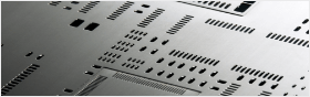
The process of printed circuit boards for designing products, material selection, technical development direction, design and processing technical specifications, can be used by printed circuit designers and craftsmen.
Different product structures have different production processes and different typesetting restrictions. For example, the gold finger board has a large layout and direction, and the test fixture or test order is different. The larger working size can meet the higher productivity, but the cost of raw materials increases a lot, and the process capability of the equipment needs to be improved. How to achieve a balance point, the design criteria and the experience of the engineers are very important.
1. the definition of processing level is not clear
The single-panel design is in the TOP layer. If you do not explain the positive and negative, you may make the board and install the device without soldering.
However, the corrections made by the pre-engineering engineers sometimes affect the characteristics or performance of the customer's products, so they have to be cautious. The PCB factory must have a set of specifications that are edited for the characteristics of the in-house process, in addition to improving product yield and improving productivity, it can also be used as a communication language with Lay-out personnel on PCB lines.
2. the large area of copper foil is too close to the outer frame
A large area of copper foil should be at least 0.2mm or more from the outer frame, because it is easy to cause the copper foil to rise and cause the solder resist to fall off when milling the shape to the copper foil.
3. draw pads with padding
Draw a pad with a pad to pass the DRC check when designing the line, but it is not suitable for processing. Therefore, the pad cannot directly generate solder resist data. When the solder resist is applied, the pad area will be covered by the solder resist, resulting in the device. Welding is difficult.
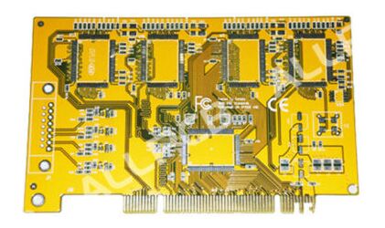
Gold finger boards have a large layout and a directional spacing, and the test fixtures or test sequences are different.
4. the electric ground layer is a flower pad and a connection
Because the design is a flower pad mode power supply, the ground layer is opposite to the actual printed board image. All the wires are isolated wires. Care should be taken when drawing several sets of power supplies or several ground isolation wires. The power supply is short-circuited and cannot cause the connection area to be blocked.
5. characters are placed
When the PCBs being on-off test, and components soldering, the legend on the silksreen layer will bring some inconvenience to the SMD pads, and if the legend height and width not big enough, the screen print will become more difficult, and if too large, the legend then will be overlapped with each other, and it is hard to be distinguished.
6. surface mount device pads are too short
This is for the on-off test. For the ultra-dense surface mount device, the distance between the two legs is quite small, and the pads are also very thin. The test pins must be placed up and down, such as the pad design is too short, although not Affects device mounting, but causes the test pin to be misplaced.
7. single-sided pad aperture setting
Single-sided pads are generally not drilled. If the holes are to be marked, the aperture should be designed to be zero. If a numerical value is designed, when the drilling data is generated, the hole coordinates appear at this position, and a problem occurs. Single-sided pads such as drilled holes should be specially marked.
8. the overlap of the pads
In the drilling process, the drill bit is broken due to multiple drilling at one location, resulting in damage to the hole. The two holes in the multi-layer board overlap, and the negative film is formed as a spacer disk, causing scrapping.
As the line density is getting higher and higher, the tolerance requirements are more and more rigorous, so the control of the film size is a major issue in many PCB factories.
The proportion of glass film using has increased. Negative film manufacturers are also actively researching alternative materials to make dimensional stability even better. For example, the dry metal film of the dry method.

9. too many filling blocks in the design or filled blocks filled with very thin lines
There is a loss of the generated light data, and the light data is not complete. Because the filling block is drawn by lines one by one during the processing of the light drawing data, the amount of light drawing data is quite large, which increases the difficulty of data processing.
10. Graphic layer abuse
Some useless connections were made on some graphics layers. The original four-layer board was designed with more than five layers, which caused misunderstanding. Violation of routine design. The graphics layer should be kept complete and clear during design.
There are several methods such as chemical precipitation of nickel gold, immersion tin, immersion silver, spray tin, electroplated nickel gold and anti-oxidation film OSP. Different metal surface treatment methods, the order of production process is different. There are also some special requirements for plating contact gold fingers or two surface treatment methods at the same time.
Generally, nickel and gold are placed after the characters, and some factories will put them before the characters to prevent the printed characters from bearing the chemical impact of the nickel-gold syrup or the thermal shock of the tin.
Immersion Sin, Immersion tin and OSP are placed after the appearance (FQC) is qualified, mainly because the protective layer formed by these three surface treatment methods is relatively delicate, easy to be artificially scratched and polluted, and can be reduced after being placed in the back step.
The electroplated nickel gold is placed in the pattern plating process, and at the same time, the tin plating process is eliminated, and the post-etching process cannot be performed after the etching.