ALLPCB


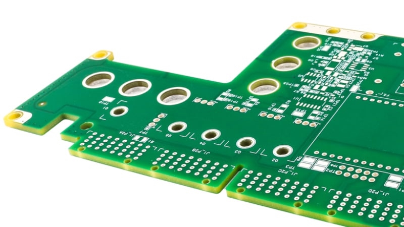
A 4 layer PCB (Printed Circuit Board) is one of the most commonly used multilayer PCBs in modern electronics. Unlike a simple 2-layer board, a four layer PCB contains four copper layers separated by insulating dielectric materials. This configuration balances performance, cost, and space efficiency, making it ideal for applications that require moderate-to-high complexity, excellent signal integrity, and reliable power delivery.
In this article, we’ll cover everything you need to know about 4 layer PCB design, 4 layer PCB stackup choices, routing strategies, manufacturing processes, and best practices. By the end, you’ll understand why the four layer board has become an industry standard for IoT devices, industrial controls, automotive electronics, and high-speed digital systems.
What is a 4-layer PCB?
A four layer PCB (Printed Circuit Board) is a type of circuit board that consists of four layers of conductive material separated by insulating layers.- Outer Layers (Top and Bottom): Used for component placement and signal routing.
- Inner Layers: Typically serve as power and ground planes, providing low-resistance return paths and EMI shielding.

Advantages of 4 Layer PCBs
Choosing a 4 layer PCB design brings several technical and commercial benefits:
- Reduced Electromagnetic Interference (EMI): Power and ground planes act as shields, reducing radiated noise.
- Improved Signal Integrity: Continuous reference planes in a 4 layer board minimize impedance discontinuities and crosstalk.
- Compact Design: Enables high-density routing, ideal for space-constrained applications.
- Improved Power Distribution: A dedicated plane in a four layer PCB ensures stable voltage and current delivery.
- Cost-Efficient for Complex Circuits: A 4 layer PCB stackup is more powerful than a 2-layer board but still cheaper than higher-layer alternatives, making it the‘sweet spot’ for many electronic products.
Applications of 4-Layer PCBs
The balance of cost, performance, and size makes four layer PCBs suitable for many industries:
- Industrial Control Systems: Controllers, PLCs, and automation modules.
- IoT Devices & Sensors: Smart home devices, wearable electronics, and remote sensors.
- Automotive Electronics: ECUs, infotainment, and driver-assist modules.
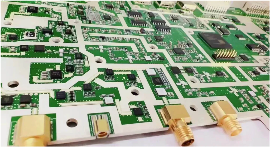
- Consumer Electronics: Smartphones, laptops, tablets, and gaming hardware.
- Communication Equipment: Routers, RF devices, and wireless modules.
Across these sectors, 4 layer PCB design enables compact yet powerful solutions.

Fundamentals of 4 Layer PCB Design
When working with a 4 layer board, engineers follow certain design principles:
- Inner Layer Use: Assigning power and ground to inner planes reduces noise and improves reference continuity.
- Outer Layer Use: Signal traces and components are placed here for accessibility.
- SMD Routing: Since components are mounted on the surface, many traces can be routed without vias, reducing complexity.
- EMI Control: Keeping return paths short and close to reference planes minimizes radiation.
A good 4 layer PCB design carefully balances manufacturability, cost, and performance.
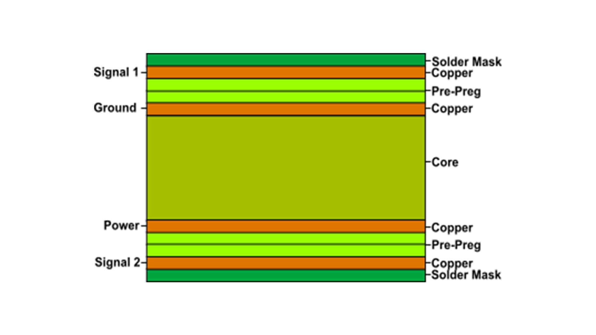
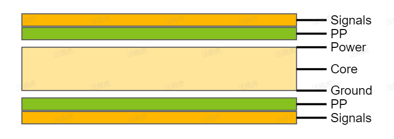
4 Layer PCB Stackup Options
The 4 layer PCB stackup is the arrangement of copper and dielectric layers. The chosen stackup directly impacts EMI, signal integrity, and manufacturability.
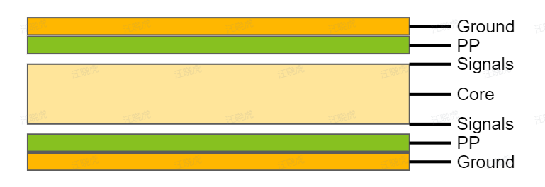
The standard 4-layer pcb stackup is as follows and GND and VCC can be switched depending on the layer with more signals.
[Signals-Ground-VCC-Signals]
Explore more: Optimizing 4-Layer PCB Layer Stackup: A Practical Guide
[Ground-Signals-Signals-Ground]
Explore more: Why need to know 4 Layer PCB Stack-up Technology?
Key Considerations for Choosing a 4 Layer PCB Stackup
- High-speed designs benefit from ground–signal–signal–ground.
- Cost-sensitive designs often use signal–ground–power–signal.
- Power delivery requirements may dictate thicker planes or higher copper weights.
By selecting the right 4-layer PCB stackup, designers ensure optimal electrical and thermal performance.
Routing principles for four layer PCB design
1. Priority Routing: Clock, differential pairs, and high-speed signals get priority.
2. Signal Layering: Keep sensitive signals close to ground planes.
3. Avoid Splits: Do not route across split planes to prevent return path discontinuities.
4. Loop Area Reduction: Smaller loops reduce EMI.
5. Length Matching: Especially critical for differential pairs and clock lines.
6. Spacing Control: Prevent crosstalk between fast and slow signals.
7. Impedance Matching: Ensure transmission lines match design requirements.
8. Power Routing: Use wide traces for current-carrying capacity.
9. Via Management: Limit via count; consider back-drilling for high-speed lines.
10. Follow Manufacturer Rules: Match design rules to ALLPCB’s fabrication capabilities.
These principles ensure that a 4 layer PCB design is both reliable and manufacturable.
Advanced Routing for High-Density 4-Layer PCBs
As devices shrink, 4 layer PCB designs often face routing challenges. Advanced strategies include:
- Length Tuning: Ensuring matched trace lengths for high-speed signals.
- Differential Pair Routing: Controlled impedance routing for pairs like USB, HDMI, or PCIe.
- Stub Minimization: Reducing stubs improves signal integrity.
- Crosstalk Mitigation: Strategic spacing and ground shielding.
Explore more: Beyond the Basics: Advanced Routing Techniques for High-Density 4-Layer PCBs
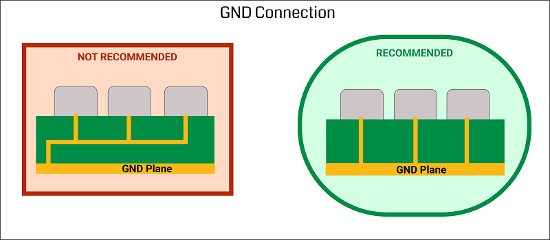
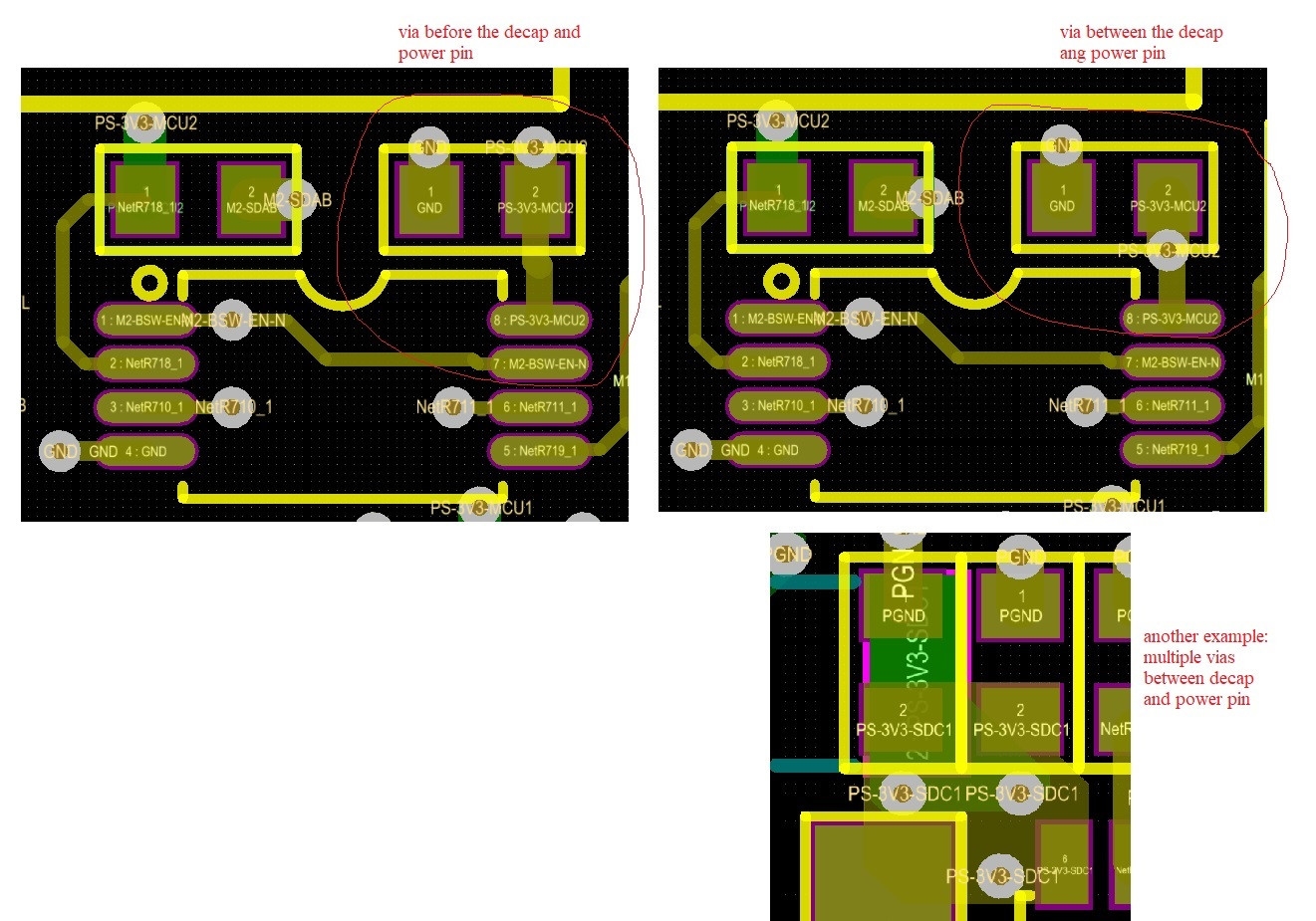
Best Practices for Via Placement in 4-Layer Boards
Via placement in a 4 layer board directly affects performance
- Avoid Excessive Transitions: Too many vias increase parasitic capacitance and inductance.
- Via-in-Pad: Improves high-frequency performance but increases cost.
- Back-Drilling: Removes stubs, reducing reflections.
- Stitching Vias: Helps maintain reference continuity and EMI shielding.
Explore more: The Ultimate Guide to Via Placement in 4-Layer PCBs: Optimizing Signal and Power Delivery
Full Overview: 4-Layer PCB Basics and FAQs
New to multilayer PCBs? This foundational guide offers insight into how 4-layer boards are structured, what benefits they offer over 2-layer options, and how design choices impact performance, cost, and prototyping time. It covers standard terminologies, common materials, and answers to frequently asked questions about stack-up, layout tools, and copper weight selection.
Read now: 4 layers PCB: Everything You Need to Know
Manufacturing Process of 4-Layer PCBs
At ALLPCB, we provide reliable four layer PCB manufacturing with customizable options.
Our Standard 4 Layer PCB Stackup Includes:
- Customizable based on board thickness (e.g., 1.6mm, 2.0mm)
- Outer copper: 1 oz or 2 oz
- Inner copper: 0.5 oz or 1 oz
- FR4 or high-Tg substrates available
We also provide DFM analysis and stackup consultation to ensure your 4 layer PCB design matches performance requirements.
Why Choose ALLPCB for Your 4 Layer Boards?
- Fast Turnaround: Same-day fabrication available
- Global Delivery: DHL, FedEx, ups, SF Express and EMS

- Engineering Support: Free 4 layer PCB stackup consultation and DFM analysis
- Competitive Pricing: No hidden fees
4 Layer PCB Prototyping options
To make four layer PCB prototyping more affordable for global engineers, ALLPCB has recently launched a special $1 campaign. You can get the PCB quote and PCBA quote for 4 layers PCB, by simply uploading your PCB files or entering your PCB specifications, such as the pcb board dimensions, quantity, etc.

Conclusion
A 4 layer PCB provides the ideal balance of cost, performance, and design flexibility. By understanding four layer PCB design rules, selecting the right 4 layer PCB stackup, and applying advanced routing techniques, engineers can achieve robust, compact, and reliable electronics.
Partnering with ALLPCB ensures your 4 layer boards are manufactured to the highest standards, with fast turnaround and competitive pricing.