


Introduction
In today's fast-evolving electronics industry, engineers face the constant challenge of packing more functionality into smaller spaces. High-Density Interconnect (HDI) Printed Circuit Boards (PCBs) have emerged as a game-changing solution, enabling compact designs without sacrificing performance. These advanced PCBs use finer traces, microvias, and innovative layering techniques to meet the demands of modern devices like smartphones, medical equipment, and automotive systems. Whether you're designing a cutting-edge wearable or optimizing an industrial IoT device, understanding HDI PCBs can unlock new possibilities for your projects. In this blog, we'll explore the key benefits of HDI PCBs, share practical design tips, and dive into the manufacturing techniques that bring these boards to life—all tailored to help engineers like you succeed.
HDI technology isn't just about shrinking board size; it's about enhancing efficiency, reliability, and signal integrity in high-performance applications. With the global HDI PCB market projected to reach $16.4 billion by 2025, growing at a CAGR of 6-8% (Report Linker), it's clear this technology is here to stay. Let's break down what makes HDI PCBs so valuable and how you can leverage them effectively in your next design.
What Are HDI PCBs?
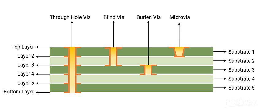
HDI PCBs are defined by their higher wiring density per unit area compared to traditional PCBs. This is achieved through features like microvias (vias with diameters of 0.006 inches or less), blind and buried vias, and finer trace widths (often below 3 mils). These characteristics allow HDI boards to support more components and connections in a smaller footprint, making them ideal for compact, high-performance electronics.
Unlike standard PCBs, which rely on larger through-hole vias and broader traces, HDI boards use advanced techniques to stack layers and route signals efficiently. For example, a typical HDI structure like 1+N+1 includes one layer of microvias on each side of a core, while more complex 2+N+2 designs add additional microvia layers for greater density. This flexibility enables engineers to reduce layer counts—say, from 10 layers in a traditional PCB to just 4 or 5 in an HDI design—without compromising functionality.
Benefits of HDI PCBs
HDI PCBs offer a range of advantages that make them indispensable for modern engineering challenges. Here's a closer look at the key benefits:
1. Miniaturization and Space Savings
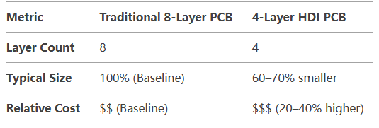
HDI technology excels at shrinking board size while maintaining or even boosting functionality. By using microvias and fine traces, engineers can place components closer together, reducing the overall footprint. For instance, an 8-layer traditional PCB can often be replaced by a 4-layer HDI board, cutting size and weight by up to 40%. This is critical for applications like smartphones, where every millimeter counts.
2. Improved Signal Integrity
Shorter signal paths in HDI designs reduce latency and signal loss. With microvias connecting adjacent layers instead of spanning the entire board, signal travel time drops significantly—sometimes by as much as 20-30% compared to through-hole vias. This is especially valuable for high-speed circuits, where maintaining impedance (e.g., 50 ohms for RF signals) is crucial to avoid reflections and crosstalk.
3. Enhanced Reliability
Microvias have a lower aspect ratio (typically 1:1 or less) than through-hole vias, making them less prone to cracking under thermal stress. Studies from the IPC show that blind and buried vias in HDI boards offer superior durability, especially in harsh environments like automotive or aerospace applications, where temperatures can swing from -40°C to 125°C.
4. Increased Design Flexibility
HDI PCBs allow more components on both sides of the board, thanks to techniques like via-in-pad and stacked microvias. This opens up routing options for complex designs, such as those with high-pin-count Ball Grid Arrays (BGAs) with pitches as low as 0.4 mm. Engineers can achieve the same functionality with fewer layers, simplifying assembly and reducing costs.
5. Cost Efficiency in the Long Run
While HDI manufacturing involves higher upfront costs due to specialized processes, the reduction in layer count and board size often offsets these expenses. For example, converting an 8-layer standard PCB to a 4-layer HDI design can cut material costs by 25-30%, making it a smart choice for high-volume production.
Design Tips for HDI PCBs
Designing an HDI PCB requires precision and foresight to maximize its benefits. Here are actionable tips to guide you through the process:
1. Prioritize Signal Integrity
For high-speed or RF designs, signal integrity is non-negotiable. Use impedance-controlled routing with trace widths and spacing calculated to match your target impedance (e.g., 100 ohms differential). Tools like Altium Designer or OrCAD X can simulate signal behavior, ensuring consistency across layers. Keep microvia stubs short—ideally under 5 mils—to minimize reflections.
2. Optimize Via Placement
Leverage blind and buried vias strategically to free up surface space. For example, placing vias in pads (via-in-pad) allows tighter component layouts, ideal for BGAs with 0.65 mm pitch or less. However, ensure proper fill (e.g., conductive epoxy) to avoid solder wicking during assembly. Staggered microvias are more reliable than stacked ones for multi-level connections, balancing cost and performance.
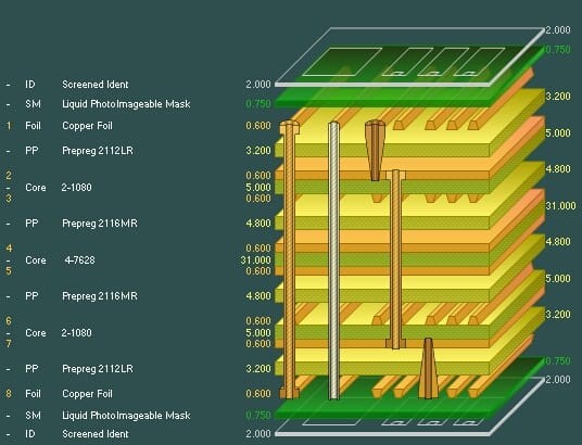
3. Plan Your Stackup Early
A well-designed stackup is the backbone of an HDI PCB. For a 1+N+1 design, use thin dielectrics (e.g., 2-3 mils) to keep microvia aspect ratios manageable. In a 2+N+2 setup, consider copper-filled stacked microvias for high-density routing, but consult your fabricator to confirm capabilities. Aim for symmetry to prevent warping—e.g., matching 1 oz copper layers on both sides.
4. Minimize Layer Count
Challenge yourself to reduce layers without sacrificing functionality. A 3-N-3 stackup (three microvia layers on each side) often strikes the sweet spot for complex designs, offering high routing density while keeping costs in check. Use routing tools to test feasibility before finalizing your design.
5. Collaborate with Your Manufacturer
HDI tolerances are tight—trace widths below 3 mils and annular rings as small as 4 mils demand precision. Share your stackup and design files with your fabricator early to verify manufacturability. For instance, laser drilling microvias requires specific dielectric materials (e.g., low-loss laminates like Rogers 4350B), which may affect lead times.
Manufacturing Techniques for HDI PCBs
Producing HDI PCBs involves specialized processes that set them apart from traditional PCB fabrication. Here's an in-depth look at the key techniques:
1. Laser Drilling for Microvias
Laser drilling is the cornerstone of HDI manufacturing, creating microvias with diameters as small as 20 microns (1 mil). Using a 355 nm UV laser, manufacturers achieve precision unattainable with mechanical drills, which struggle below 6 mils. This process supports high-density layouts by forming vias that connect only adjacent layers, leaving other layers free for routing.
2. Sequential Lamination
Unlike standard PCBs, which are laminated in one step, HDI boards often undergo multiple lamination cycles. For a 2+N+2 design, the core is laminated first, followed by additional layers with microvias drilled and plated in sequence. This builds up the structure layer by layer, ensuring alignment within 2-3 mils to avoid registration errors.
3. Via Filling and Plating
After drilling, microvias are filled with conductive (e.g., copper) or non-conductive epoxy to create a flat surface for component mounting. Copper plating follows, typically via electroless deposition, to ensure reliable electrical connections. For via-in-pad designs, this step is critical to prevent voids, requiring fill depths of at least 80% of the via height.
4. Advanced Imaging and Etching
HDI boards demand finer lines (e.g., 2-3 mils) than traditional PCBs (5-8 mils), so manufacturers use Laser Direct Imaging (LDI) instead of conventional photolithography. LDI offers resolution down to 1 mil, ensuring crisp trace patterns. Wet etching then removes excess copper, with tight process controls to maintain uniformity within ±0.5 mils.
5. Surface Finishing
To protect fine features and ensure solderability, HDI PCBs often use finishes like Electroless Nickel Immersion Gold (ENIG). ENIG provides a flat, corrosion-resistant surface with a gold layer of 2-5 microinches, ideal for fine-pitch components. Alternatives like Immersion Silver suit high-frequency designs due to lower signal loss.
Challenges and Solutions in HDI PCB Design and Manufacturing
While HDI PCBs offer immense benefits, they come with challenges that engineers must address:
Challenge 1: Higher Costs
The use of laser drilling, thin materials, and multiple lamination cycles increases production costs by 20-30% compared to standard PCBs. Use our HDI PCB price calculator to estimate the cost of your projects.
Solution:
Optimize your design to minimize layer count and microvia usage. A 3-N-3 stackup, for instance, balances cost and density effectively.
Challenge 2: Complex Design Process
Tight tolerances and dense layouts require advanced skills and software. A misaligned via (e.g., off by 5 mils) can ruin a board.
Solution:
Use design tools with HDI-specific features, like Altium Designer's microvia routing, and validate with Design for Manufacturability (DFM) checks.
Challenge 3: Thermal Management
More components in a smaller area generate heat, risking performance drops at temperatures above 85°C.
Solution:
Incorporate thermal vias and copper planes to dissipate heat, a thermal resistance below 10°C/W for critical areas.
How ALLPCB Supports HDI PCB Projects
For engineers tackling HDI designs, partnering with a reliable manufacturer is key to success. At ALLPCB, we specialize in quick-turn prototyping and advanced manufacturing, delivering HDI PCBs with trace widths as fine as 2 mils and microvias down to 3 mils in diameter. Our global logistics ensure fast delivery—while our expertise in sequential lamination and laser drilling guarantees precision for even the most complex stackups. Whether you're refining66 a 1+N+1 design or pushing the limits with an any-layer interconnect, we provide the tools and support to bring your vision to life efficiently and cost-effectively.
Conclusion
HDI PCBs are revolutionizing electronics by offering unmatched miniaturization, signal performance, and design flexibility. From reducing a 10-layer board to a 4-layer marvel to boosting reliability in extreme conditions, the benefits are clear. By following design tips like optimizing via placement and planning stackups carefully, engineers can harness these advantages fully. Meanwhile, manufacturing techniques like laser drilling and sequential lamination ensure these designs become reality with precision and quality.
As devices continue to shrink and performance demands soar, HDI technology will only grow in importance. Whether you're designing for consumer electronics, automotive systems, or medical devices, mastering HDI PCBs equips you to stay ahead in this competitive field. Ready to start your next HDI project? Dive in with confidence, knowing you have the knowledge—and the right manufacturing partner—to succeed.