


In today's fast-paced electronics industry, the demand for smaller, faster, and more efficient devices is relentless. From smartphones that fit in your pocket to wearable health monitors, engineers face the challenge of packing more functionality into less space. At the heart of this revolution lies microvia technology—a game-changer in printed circuit board (PCB) design. Microvias, tiny laser-drilled holes that connect layers in high-density interconnect (HDI) PCBs, enable the miniaturization that modern devices depend on. In this blog, we'll explore how microvia technology works, why it's critical for compact electronics, and how it addresses the practical needs of engineers pushing the boundaries of innovation.
Miniaturization isn't just a trend—it's a necessity. As devices shrink, traditional PCB designs with large through-hole vias struggle to keep up. Microvias solve this by offering a smaller footprint, higher connection density, and improved electrical performance. Whether you're designing a cutting-edge medical implant or a 5G-enabled gadget, understanding microvias can unlock new possibilities. Let's dive into the details and see how this technology shapes the PCBs of tomorrow.
What Are Microvias?
Microvias are small vias—typically less than 150 microns (0.15 mm) in diameter—used to connect adjacent layers in multilayer PCBs. Unlike traditional plated through-holes that span the entire board thickness, microvias are shallow, with a depth-to-diameter aspect ratio of 1:1 or less, and a maximum depth of 0.25 mm, as defined by IPC standards. These tiny holes are usually created using laser drilling, allowing for precision that mechanical drills can't achieve.
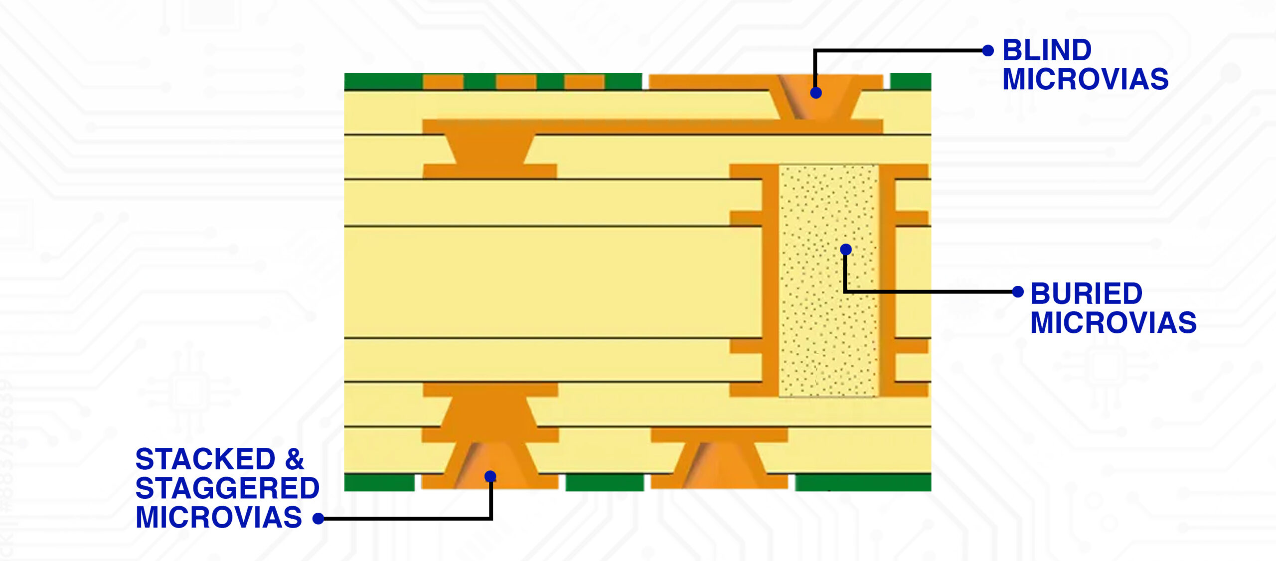
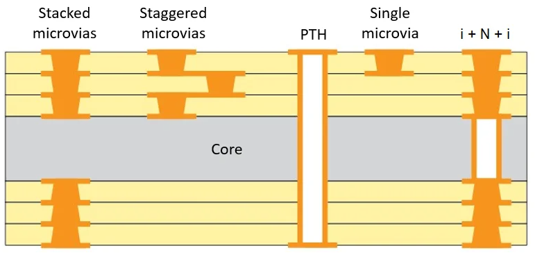
What sets microvias apart is their role in HDI PCBs. They come in two main types: blind microvias, which connect an outer layer to an inner layer, and buried microvias, which link inner layers without reaching the surface. Stacked or staggered configurations further enhance their versatility, enabling complex interconnections in tight spaces. For engineers, this means more components and traces can fit on a single board without increasing its size.
The Role of Microvias in Miniaturization
Miniaturization hinges on one key principle: maximizing functionality per square millimeter. Microvias make this possible by shrinking the real estate needed for interlayer connections. Traditional vias, often 0.3 mm or larger in diameter, consume valuable space and limit trace routing options. In contrast, microvias as small as 50 microns free up room for finer traces—down to 25 microns (0.025 mm)—and denser component layouts.
Consider a modern smartphone: it integrates processors, memory, sensors, and wireless modules into a device thinner than 8 mm. Without microvias, fitting these components onto a single PCB would require a larger board or multiple boards, increasing size and weight. By using stacked microvias in an HDI design, engineers can achieve layer counts of 10 or more while keeping the board compact. This density is why HDI PCBs with microvias are standard in consumer electronics, automotive systems, and aerospace applications.
Beyond size, microvias reduce layer count. A traditional multilayer PCB might need 12 layers to route signals, while an HDI PCB with microvias could accomplish the same in 6 or 8 layers. Fewer layers mean lower material costs and simpler manufacturing—key considerations for cost-conscious engineers.
How Microvias Enhance Electrical Performance
Size isn't the only advantage microvias bring to the table—they also boost electrical performance. In high-speed circuits, signal integrity is critical, and microvias deliver by shortening signal paths. A typical through-hole via might span 1.6 mm across a board, introducing parasitic capacitance and inductance that degrade signal quality at frequencies above 1 GHz. Microvias, with depths often below 0.1 mm, minimize these effects, supporting signal speeds up to 25 Gbps or higher in 5G and data center applications.
Impedance control is another benefit. Fine traces paired with microvias allow engineers to maintain consistent impedance—say, 50 ohms for single-ended signals or 100 ohms for differential pairs—across the board. This precision reduces signal reflections and crosstalk, which are common headaches in high-frequency designs. For example, in a 5G antenna module, microvias ensure clean signal transmission between layers, enhancing overall system reliability.
Microvia Fabrication: Precision Matters
Creating microvias isn't as simple as drilling a hole—it's a high-tech process that demands accuracy. Laser drilling, typically using CO2 or UV lasers, is the go-to method. These lasers can ablate dielectric materials like FR-4 or polyimide with pinpoint precision, forming holes as small as 25 microns. After drilling, the holes are plated with copper via electroless deposition and electroplating to ensure reliable electrical connections.
The process isn't without challenges. Aspect ratios above 1:1 risk incomplete plating, leading to weak connections or voids. For instance, a 100-micron-diameter microvia with a 150-micron depth (1.5:1 ratio) might suffer plating defects, reducing reliability. Engineers must balance hole size and depth, often sticking to 0.8:1 or lower for robust results. Material choice also matters—high-Tg (glass transition temperature) laminates like Rogers 4350B withstand laser heat better than standard FR-4, minimizing damage during fabrication.
Stacked microvias, where multiple microvias align vertically, add complexity. Research shows that stacks of three or more can fail under thermal stress due to coefficient of thermal expansion (CTE) mismatches between copper (17 ppm/°C) and dielectric (50-70 ppm/°C). Staggered microvias, offset between layers, often prove more reliable for high-layer-count designs.
Applications Driving Microvia Adoption
Microvia technology shines in applications where size, weight, and performance are non-negotiable. In consumer electronics, devices like smartwatches rely on HDI PCBs with microvias to cram processors, batteries, and displays into wrist-sized packages. A typical smartwatch PCB might use 6 layers with 75-micron microvias, achieving a thickness under 0.8 mm.
In the automotive world, advanced driver-assistance systems (ADAS) depend on microvias for compact radar and camera modules. These systems operate at frequencies around 77 GHz, where signal loss from long vias would degrade performance. Microvias keep connections short and signals strong, fitting everything into tight dashboard spaces.
Medical devices, such as pacemakers, push miniaturization to the extreme. A pacemaker PCB might measure just 20 mm x 20 mm, using 50-micron microvias to connect 8 layers. This density supports critical functions like heart rhythm monitoring while meeting strict reliability standards—failure isn't an option here.
Challenges and Trade-offs with Microvias
While microvias offer big advantages, they come with trade-offs engineers must navigate. Cost is a major factor—laser drilling and HDI fabrication are more expensive than traditional mechanical drilling. A 4-layer HDI board with microvias might cost 20-30% more than a standard multilayer PCB, depending on volume and complexity.
Reliability is another concern. Thermal cycling—say, from -40°C to 85°C in automotive testing—can stress microvia junctions. Studies indicate that 2-level stacked microvias withstand 20 times more cycles than 4-level stacks before cracking. For high-reliability applications, engineers might opt for staggered designs or limit stacking to two levels, trading some density for durability.
Design complexity also rises. Routing traces around microvias requires tighter tolerances, often below 3 mils (0.076 mm), pushing the limits of standard PCB design tools. Engineers need advanced software and close collaboration with fabricators to avoid costly rework.
The Future of Microvia Technology
As electronics evolve, microvias will keep pace. The rollout of 6G networks, expected by 2030, will demand even higher frequencies—up to 300 GHz—where microvias' short paths will be indispensable. Wearable and implantable devices will push for smaller vias, potentially down to 15 microns, enabled by next-gen lasers and materials like liquid crystal polymer (LCP).
Sustainability is also on the horizon. Researchers are exploring biodegradable dielectrics and lead-free processes to make HDI PCBs greener. Meanwhile, AI-driven design tools could optimize microvia placement, cutting costs and boosting performance. For engineers, staying ahead means embracing these trends while mastering today's techniques.

How ALLPCB Supports Microvia Innovation
For engineers tackling microvia-based designs, partnering with a capable manufacturer is key. Whether you're building a compact IoT device or a high-speed telecom system, we provide the precision and support to bring your ideas to life.
Conclusion
Microvia technology is more than a tool—it's a cornerstone of modern PCB design. By enabling miniaturization, enhancing performance, and supporting cutting-edge applications, microvias empower engineers to meet the demands of an ever-shrinking, high-speed world. Yes, they bring challenges like cost and complexity, but the payoffs in density and efficiency are worth it. As devices get smaller and smarter, microvias will remain at the forefront, driving innovation one tiny hole at a time. Ready to shrink your next design? The power of microvias is in your hands.