


PCB Fabrication + Component Sourcing + Assembly + Testing – All in One Place
ISO 9001, IPC-A-610 Class 2/3 Standards, 100% AOI & X-Ray Testing
DFM/DFA Analysis, BOM Optimization, and Design Guidance
Access to 1000+ suppliers, BOM optimization, and risk mitigation
SMT, THT and Mixed assembled technology
Single/Double sided assembly
Lead-free (RoHS compliant)
Low-Temperature Soldering for Flex PCBs
Box Build Assembly
01005 chip size
0.3mm BGA spacing
0.25mm fine-pitch ICs
Automotive-Grade Components (AEC-Q Certified)
Turnkey, Consigned, Partial Turnkey
Rigid, Flex PCB, Rigid-Flex PCB
HDI with Blind/Buried Vias (Up to 32 Layers)
Ceramic/Metal-Core Substrates
RF/Microwave PCBs (±5% Impedance Control)
20+ SMT Lines (Prototype to Mass Production)
Daily Capacity: 10M SMT Joints, 180K DIP Joints, 50+ Designs
High-Precision Siemens SMT, GKG-G5 SPI, EAGLE 3D AOI
AI-Driven Dynamic Production Scheduling
MES System for Real-Time Yield Monitoring
Partnerships with 1.000+ verified suppliers (Original manufacturers and authorized distributors)
Exclusive Channels for Critical Components (e.g., Automotive MCUs)
Real-Time Market Risk Mitigation
Professional BOM optimization including alternates, lifecycle alerts, and cost-down suggestions
Reduce BOM costs by 15-30% through cross-industry bulk purchasing
MOQ optimization reduces excess inventory by 40%
24-Hour BOM Review & Component Matching
Intelligent Alternate Part Recommendations (>99% Compatibility)
Emergency Order Service (72-Hour Global Delivery)
Smart Warehouse (300K+ SKUs, Humidity/ESD Controlled)
JIT(Just in time) Inventory for Cost Reduction
Safety Stock Alerts for Critical Components
Free DFM/DFA Analysis and 24H customer support
Live dashboard: Real-time yield rate (≥99.2%) & station alerts
IC Programming, Functional Testing
Flying Probe/fixture testing
IQC, SPI, Online AOI, Offline AOI, IPQC, X-Ray
IC programming, functional test
Monthly Quality Reports (CPK ≥1.67)
6 Sigma Process Optimization
Full-Process SPC Data Transparency
ISO 9001/14001/45001/13485, IATF 16949, UL Certified
IPC-A-610 Class 2/3 Standards
Customized QCP (Quality Control Plan)
24-Hour Prototyping (1–50pcs)
Small Batch (<500pcs) in 3 Days
Mass Production (Daily 10M+ Joints)
In-House Logistics, DHL/FedEx, DDP
Smart Customs Clearance (<2 Hours)
PCB-PCBA <300m distance: Panel→assembly in 4hr
Real-Time Tracking
Live system monitoring ensures 98% on-time delivery rate
Contingency Plans for Extreme Scenarios
Response within 2 hours
Provide solutions within 2 days
Monthly report and improve
From online quote system or emails, response quickly
Via Email, Skype/Whatsapp or phone
DFM check, BOM optimization, and design guidance
Global component network, Full-process system monitoring
20+ Siemens high precision SMT machines, first sample test
X-Ray testing, functional test and final inspection
Shield bag packaging, DHL/FEDEX/UPS shipping
The professional support team responds complaints within 2 hours and provides immediate solutions
How ALLPCB assembly factory process and what kind of benefits for our customers
 Design Review & DFM Analysis
- Engineers validate PCB design files (Gerber, BOM, CPL) against manufacturing capabilities.
- Perform Design for Manufacturability (DFM) checks for component spacing, pad sizes, and thermal management.
- Risk Mitigation: Prevents costly redesigns by flagging layout errors (e.g., solder bridges, insufficient clearances).
- Cost Optimization:Recommends design tweaks to reduce material waste and improve yield rates.
- Compliance: Ensures adherence to IPC standards (e.g., IPC-A-610) for industry-grade quality.
 Component Procurement & Verification
- Source components from certified suppliers using real-time inventory databases.
- Authenticate parts via batch-code tracing, X-ray inspection, or third-party lab testing.
- Genuine Parts Guarantee: Eliminates counterfeit risks with supplier audits and COC (Certificate of Conformance).
- Supply Chain Resilience: Multi-sourcing strategies prevent delays for obsolete or long-lead-time components.
- Cost Transparency: Price-match commitments and bulk-order discounts.
 Solder Paste Printing
- Use a stencil and precision printer to evenly coat solder paste on PCB pads.
- Adjust printing parameters (pressure, speed) to ensure solder paste thickness and coverage accuracy.
- The basis of welding quality: accurate solder paste quantity reduces defects such as cold solder joints or bridging.
- Process stability: parameter standardization ensures consistency in batch production.
 Solder Paste Inspection (SPI)
- Detect solder paste thickness, volume and position deviation through 3D optical scanning.
- Real-time feedback data to calibrate printer parameters.
- Defect prevention: intercept solder paste anomalies before soldering to avoid subsequent rework.
- Process control: digital monitoring improves process capability (CPK).
 SMT Assembly
- Apply solder paste via stencil printing.
- Place components using high-precision pick-and-place machines.
- Reflow soldering in controlled-temperature ovens.
- Precision: ±0.025mm placement accuracy for 0201 packages and micro-BGAs.
- Process Control: Solder paste inspection (SPI) and AOI (Automated Optical Inspection) ensure defect rates <0.1%.
- Traceability: Barcode tracking for every PCB panel.
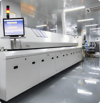 Reflow Soldering
- The temperature curve is set according to the characteristics of the solder paste, divided into three stages: preheating, reflow, and cooling.
- Precisely control the peak temperature (usually 220–250°C) to form reliable solder joints.
- Welding reliability: avoid cold welding or overheating to ensure the stability of electrical connections.
- Consistency: Temperature curve monitoring ensures uniform soldering quality for each batch.
 First sample testing
- Perform electrical tests (such as ICT) and basic functional verification on the first sample.
- Compare with design specifications and confirm key parameters (voltage, signal integrity).
- Early risk exposure: Discover design or process problems in the early stages of production.
- Fast iteration: Reduce rectification costs after mass production.
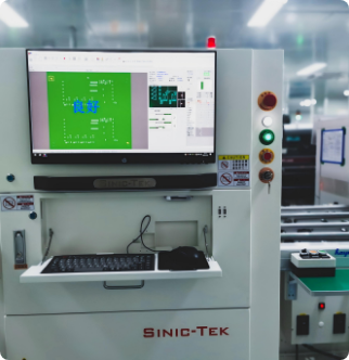
 Automated Optical Inspection (AOI)
- Detect solder joint quality, component offset or polarity errors through multi-angle cameras.
- Machine learning algorithms automatically classify defects (such as missing parts and tombstones).
- Comprehensive inspection: Covers more than 99% of visible defects and reduces manual omissions.
- Quality dataization: Generates inspection reports to support continuous process optimization.
 Through-Hole Component Soldering
- Insert leads into drilled holes manually or via automated insertion machines.
- Wave soldering or selective soldering for robust connections.
- Durability: Mechanical strength testing for high-stress applications (e.g., automotive, industrial).
- Consistency: Automated systems eliminate human error in pin alignment.
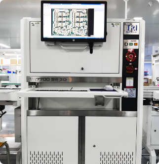
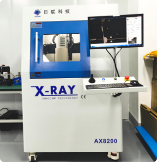 X-Ray Inspection
- Use X-ray fluoroscopy to detect hidden solder joints (such as BGA, QFN).
- Analyze whether the solder joint bubble rate and filling integrity meet IPC standards.
- Non-destructive testing: Ensure the internal quality of invisible solder joints.
- High-precision analysis: Quantify defect indicators (such as bubble rate <25%) to ensure long-term reliability.
 Testing & Functional Validation
- Perform environmental testing (high and low temperature, vibration), aging testing and full functional verification.
- Simulate terminal usage scenarios to ensure stable operation of the product in actual applications.
- Performance compliance: 100% meets customer specifications.
- Durability assurance: Verify product life cycle through accelerated life testing.
 Final Inspection & Packaging
- Visual inspection under magnification for cosmetic flaws.
- Anti-static ESD packaging with moisture barrier bags.
- Labeling and serialization for logistics tracking.
- Aesthetic Standards: Reject boards with scratches, discoloration, or misalignment.
- Shipping Safety: MIL-STD-2073-compliant packaging to prevent transit damage.
- Delivery Tracking: Real-time logistics updates via integrated courier APIs.