

● 1 Layer PCB vs 2 Layer PCB
● 2 Layer PCB vs 4 Layer PCB
Instant Quote
Full feature prototype PCB custom service at low cost.
Flexible PCB
Customized FPC service with high standards
Rigid-Flex PCB
High precision rigid-flex PCB customized service
PCB Assembly Quote
Leading assembly factory with Siemens production line
SMD Stencil
Laser cutting high precision stencil service
1 layer pcb, 2 layer pcb and 4 layer pcb are very common 3 types of pcb board in pcb manufacturing. When and where are they generally used? What are the differences between them. In this articel, we will not tell the 2 layer pcb thickness, but tell the detailed introduction for 2 layer pcb vs 4 layer pcb. Besides, there is a tutorial about 2 layer pcb board making.


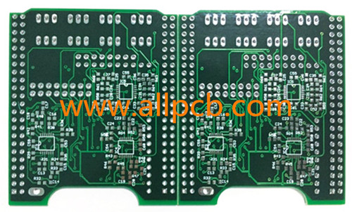
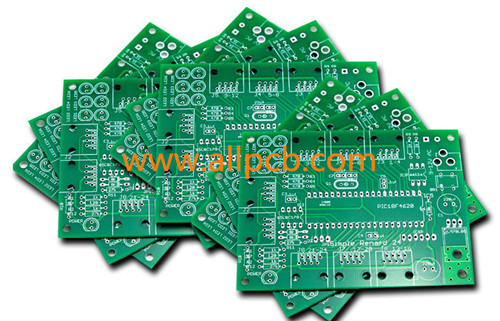
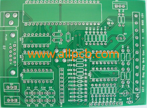
1 Layer PCB has only one layer of conductive material and is suitable for low density and simple design. 2 Layer PCB contains 2 layers and layout is easier for more traces. The 2-layer PCB provides more surface area for housing a conductor pattern. Its surface is two times larger than that of a 1 layer PCB.

For a hobbyist or student, you’d better choose to make 1 layer PCB by yourself. Because 1 layer pcb is much easier to do. 2 layer PCB is a little harder. So we suggest you can get your 2 layer pcb boards made commercially by PCB manufacturer, such as ALLPCB.com. It takes only &10 for 5pcs 2 layer pcb boards in 24 hours with free shipping!
The 2 layer PCB is the most common used among all the multilayer PCBs. It can accommodate interconnects on both sides. Signal integrity and interference levels weigh in the favor of 4-layer pcb boards. But, what are the differences between 2 layer and 4 layer PCB?
The 2-layer PCB stackup contains 1 top layer and 1 bottom layer. The 4 layer PCB stackup contains ont only the top layer and bottom layer, but also 2 inner layers - inner layer 1 and inner layer 2. Between layers there is prepreg.

Standard 4 Layer PCB Stackup
Vias in 2 layer PCB are used to create electrical connections that enable the routing of the traces so that they reach the opposite side of the board. Even more surface area is available for traces in a 4 layer PCB design than that in a 2 layer PCB. The 4 layer PCB design involves a prepreg layer that bonds two layers and a double-sided boards together by applying heat and pressure. Prepreg provides dielectric between the layers.
If the microstrip traces comprising a ground plane are utilized, the 2 layer PCB delivers more functionality as there are no propagation delays or other problems. However, a 4-layer PCB design consisting of ground and VCC plane layers and 2 signal layers is more preferred. This design struggle with impedance and propagation delays.
Due to complexity of design, higher sensitivity, the higher levels of signal integrity and reduced interference levels, the 4 layer PCB is more expensive than a 2 layer PCB. The price of 2 layer PCB can be as low as $2/piece, and the cost of 4 layer pcb can be as low as $6.5/piece in ALLPCB.com.
The After your payment, your 2 layer pcb order with standard manufacturing specifications can be shipped within 24 hours and the lead time of your 4 layer pcb order can be within 48 hours on ALLPCB.com. Order now, we offer worldwide free shipping service!
Specifications | 1 Layer PCB | 2 Layer PCB | 4 Layer PCB |
Price | $2/piece | $2/piece | $13/piece |
Lead Time | 24 Hours Turn | 24 Hours Turn | 48 Hours Turn |
Max Board Size | 650x520mm | 650x520mm | 650x500mm |
Min. Order Quantity | 5 | 5 | 5 |
Material | FR-4 Shengyi TG140 | FR-4 Shengyi TG140 | FR-4 Shengyi TG140 |
Finished Copper (outer) | I oz. Cu. | I oz. Cu. | I oz. Cu. |
Board Thickness | 1.6mm | 1.6mm | 1.6mm |
Solder Mask(TAIYO) | Green Mask | Green Mask | Green Mask |
Silkscreen Color(TAIYO) | White Legend | White Legend | White Legend |
Surface Finish | HASL with Lead | HASL with Lead | HASL with Lead |