

● Photo printing
● Screen printing
Instant Quote
Full feature prototype PCB custom service at low cost.
Flexible PCB
Customized FPC service with high standards
Rigid-Flex PCB
High precision rigid-flex PCB customized service
PCB Assembly Quote
Leading assembly factory with Siemens production line
SMD-Stencil
Laser cutting high precision stencil service
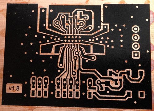
Image transfer basically involves the transfer of the conductor pattern from the film master on to the copper clad base material or any other metal clad laminate. Image transfer is to affix to or coat with a layer of photosensitive film on the surface of copper. Under the irradiation of ultraviolet rays, the film on the film pattern transfers to the surface of copper, and forms a resist mask pattern. Which is not protected by the etchant, will be etched in a subsequent chemical etch process, and the resist film is removed after the etching process to obtain the desired bare copper circuit pattern. In PCB manufacturing, the two methods common for image transfer are photo printing and screen printing.

PCB Image Transfer
1. Photo printing
Photo printing is a very precise process, which is generally used in the manufacture of semiconductors and integrated circuits, where the width of the conductor is usually in the region of a few microns. While such precision technology is not required for general PCB production, the 100μm conductor width requirements and printed circuit board are used in professional photo printing processes.
2. Screen printing
Less accurate than the photo printing, but screen printing is still a relatively cheap and simple method in PCB manufatcure. And the majority of PCBs produced worldwide are screen printing for its low cost and simplicity.