

● The Benefits of Etch a PCB by Yourself
● Some Issues While Etching PCB
● Protect Yourself While Etching PCB
● How to Etch a PCB
● Types of PCB Etching Process
● Some Examples of PCB Etching Process
Instant Quote
Full feature prototype PCB custom service at low cost.
Flexible PCB
Customized FPC service with high standards
Rigid-Flex PCB
High precision rigid-flex PCB customized service
PCB Assembly Quote
Leading assembly factory with Siemens production line
SMD-Stencil
Laser cutting high precision stencil service
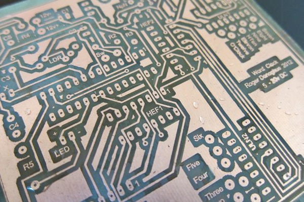
PCB etching process is one of the major steps in the chemical processing of subtractive printed circuit board. It is the removal of copper, to achieve the desired circuit patterns. In PCB etching process, all copper is removed except the circuitry that is protected by the tin plating applied during the previous treatment in PCB manufacture. The tin is then stripped and the copper is cleaned and the newly prepared circuit is ready for solder mask.

PCB Etching Process
It is easy and fun to etch small number of simple pcb boards by yourself at home.
1. The Benefits of Etch a PCB by Yourself:
No MOQ - You can make no matter how many pieces pcb boars you want
It takes less time than to order from a pcb manufacturer
It is really fun and rewarding for hobbyists
However, it may occur some issues during the pcb etching process, and because of dangerous chemicals and power tools, you should protect yourself by some methods.
2. Some Issues While Etching:
There is a risk of injuries due to the chemicals involved
The quality may not be as good as expected at the first time, such as over-etching
You may be a problem of toxic chemicals waste disposal
3. Protect Yourself While Etching:
Wear gloves, protection glasses, and an apron during the whole process
Work near an emergency eyewash station
Prepare a first aid box and a phone in advance
4. How to Etch a PCB
If you’re interested in etching pcb boards, you can watch this video, which will tell you how to etch a PCB. We hope it can help you go more smoothly.
5. Types of PCB Etching Process
Typically, the PCB etching process can be divided into two types: chemical etch and laser etch.
Chemical Etch
Chemical etching is usually done with ammonium per sulphate or ferric chloride
For PTH (Plate-through Hole), additional steps of electroless deposition are done after the holes are drilled, then copper is electroplated to build up the thickness, the boards are screened, and plated with tin/lead. The tin/lead becomes the resist leaving the bare copper to be etched away.
Laser Etch
A new process creating new standards and the demise of the chemical process is plasma etch. In addition to no etch-back, this process also eliminates imaging, or film error using a direct imaging process, which transfers the layer image directly to the material.
6. Some Examples of PCB Etching Process:
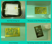
Example 1


Example 2
Step 1. Masking the Board

Step 2. Etching the Board

Step 3. Removing the Resist
Step 4. Finishing Touches

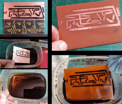
Example 3
Step 1. Transfer the Layout to the Board

Step 2. The Etching Process
Etching Process
