If you're diving into PCB design, you might be wondering about the difference between non-plated through-holes (NPTH) and plated through-holes (PTH). Simply put, NPTH are holes drilled through a printed circuit board without a conductive coating, often used for mechanical purposes, while PTH have a conductive layer inside, enabling electrical connections between layers. This guide will break down the key differences, advantages, and disadvantages of NPTH and PTH, focusing on aspects like PCB reliability, electrical conductivity, and cost comparison. Whether you're a beginner or a seasoned engineer, you'll find practical insights to help with your next project.
Introduction to Through-Holes in PCB Design
Through-holes are a fundamental part of printed circuit board (PCB) design. These are holes drilled from the top to the bottom of the board, serving various purposes depending on whether they are plated or non-plated. Understanding the role of non-plated through-holes (NPTH) versus plated through-holes (PTH) is crucial for designing efficient and reliable PCBs. In this blog, we'll explore how NPTH and PTH differ, their specific uses, and why one might be better suited for your project than the other. We'll also cover key factors like cost, reliability, and electrical performance to guide your decision-making process.
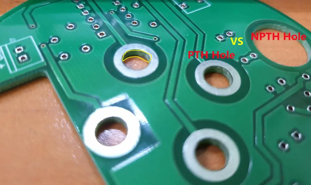
What Are Non-Plated Through-Holes (NPTH) and Plated Through-Holes (PTH)?
Non-Plated Through-Holes (NPTH)
Non-plated through-holes are holes drilled through a PCB that do not have a conductive coating on their inner walls. These holes are typically used for mechanical purposes, such as mounting the board to a chassis or enclosure with screws or standoffs. Since they lack a conductive layer, NPTH do not facilitate electrical connections between layers or components. They are purely structural, providing support or alignment in the design.
Plated Through-Holes (PTH)
Plated through-holes, on the other hand, are holes with a thin layer of conductive material, usually copper, coated on their inner walls. This plating allows electrical signals to pass between different layers of a multilayer PCB or to connect components mounted on the board. PTH are essential for through-hole component mounting, where component leads are inserted into the holes and soldered in place, ensuring both mechanical stability and electrical connectivity.
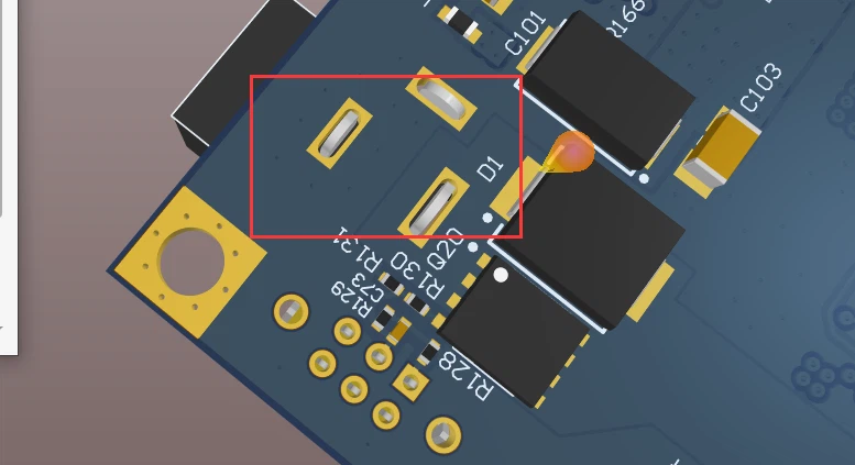
Key Differences Between NPTH and PTH
While both NPTH and PTH are through-holes, their purposes and characteristics vary significantly. Here's a breakdown of the main differences:
- Purpose: NPTH are used for mechanical support, such as mounting or alignment, while PTH are used for electrical connections and component mounting.
- Conductivity: NPTH have no conductive material and do not support electrical signals, whereas PTH have a conductive coating for signal transmission.
- Manufacturing Process: NPTH are simpler to produce since they don't require plating, while PTH involve an additional electroplating step to deposit copper inside the hole.
- Cost: NPTH are generally cheaper due to the simpler manufacturing process, while PTH add to production costs because of the plating process.
Understanding these differences is the first step in choosing the right type of through-hole for your PCB design. Let's dive deeper into the specific advantages and disadvantages of each, focusing on non-plated through-holes versus plated through-holes.
NPTH Advantages in PCB Design
Non-plated through-holes offer several benefits, especially in specific applications where electrical conductivity is not required. Here are some key NPTH advantages:
Cost-Effectiveness
One of the biggest advantages of NPTH is their lower cost. Since they do not require the additional step of electroplating with copper, the manufacturing process is simpler and less expensive. For projects where budget is a concern and mechanical mounting holes are needed, NPTH can save significant costs. For example, in a basic two-layer PCB design, using NPTH for mounting can reduce production expenses by up to 10-15% compared to unnecessary PTH in those positions.
Simplified Manufacturing
Without the need for plating, NPTH can be drilled and left as-is during the PCB fabrication process. This reduces the number of steps and potential points of failure during manufacturing, leading to faster production times. For high-volume production runs, this simplicity can translate into quicker turnaround times.
Mechanical Strength for Mounting
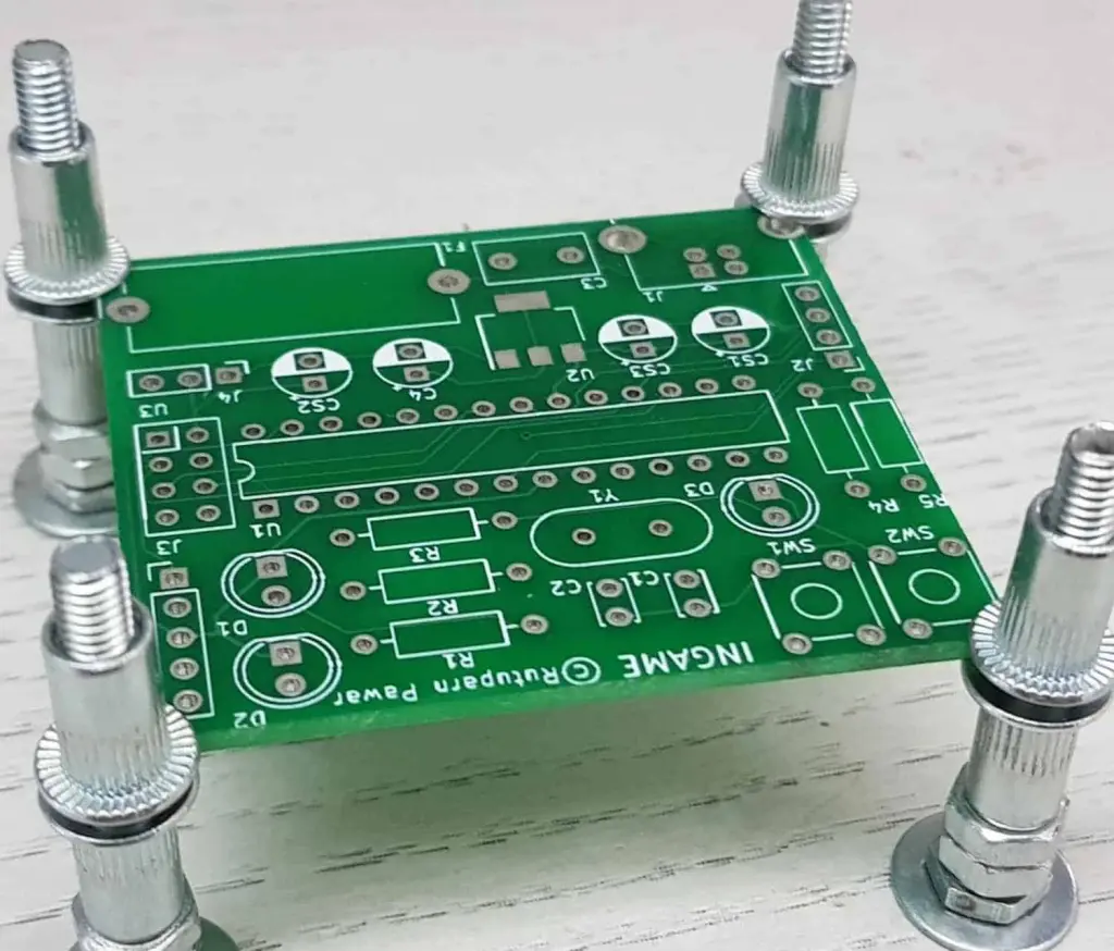
NPTH are ideal for applications where mechanical strength is needed. They provide robust mounting points for screws, bolts, or standoffs, ensuring the PCB is securely fastened to an enclosure or frame. Since there's no conductive material, there's also no risk of unintended electrical shorts at mounting points, which can be a concern with PTH if not properly insulated.
PTH Disadvantages in PCB Design
While plated through-holes are essential for many designs, they come with certain drawbacks that might make NPTH a better choice in specific scenarios. Here are some notable PTH disadvantages:
Higher Manufacturing Costs
The electroplating process required for PTH adds to the overall cost of PCB production. This process involves depositing a layer of copper inside the drilled holes, which requires additional materials, time, and specialized equipment. For a multilayer PCB with hundreds of PTH, this can increase costs by 20-30% compared to a similar design using NPTH where possible.
Complexity in Fabrication
The plating process introduces additional complexity to PCB manufacturing. Issues like uneven plating or insufficient copper thickness can lead to reliability problems, such as poor electrical connections or weak mechanical bonds. For instance, if the copper layer inside a PTH is less than 25 micrometers thick, it may not withstand the thermal stress of soldering, leading to cracks or failures.
Potential for Electrical Issues
PTH can sometimes cause unintended electrical issues if not designed or insulated properly. For example, in high-voltage applications, a PTH used near a mounting point could create a risk of arcing or short-circuiting if debris or moisture accumulates. NPTH, being non-conductive, eliminate this risk entirely in mechanical applications.
Comparing PCB Reliability: NPTH vs. PTH
Reliability is a critical factor in PCB design, as it directly impacts the performance and lifespan of the final product. Let's compare how NPTH and PTH stack up in terms of PCB reliability.
NPTH Reliability
For mechanical purposes, NPTH are highly reliable. They provide strong, stable mounting points without the risk of electrical failure since they aren't part of the circuit. Their simplicity also means fewer manufacturing defects, as there's no plating to worry about. In harsh environments, such as those with high vibration or thermal cycling, NPTH maintain their integrity as long as the board material itself holds up.
PTH Reliability
PTH reliability depends on the quality of the plating and the design of the PCB. A well-manufactured PTH with a uniform copper thickness of at least 25-30 micrometers can be very reliable, supporting electrical connections through multiple layers. However, poor plating can lead to issues like barrel cracking under thermal stress or insufficient conductivity, causing signal loss. In a study of multilayer PCBs, it was found that up to 5% of PTH failures were due to plating defects during thermal cycling tests at 125°C.
In summary, NPTH are more reliable for mechanical tasks, while PTH reliability hinges on precise manufacturing and design considerations.
Electrical Conductivity: NPTH vs. PTH
Electrical conductivity is a key consideration when choosing between NPTH and PTH, as it directly affects how signals and power are transmitted in a PCB.
NPTH and Electrical Conductivity
Since NPTH lack any conductive material, they play no role in electrical conductivity. They are strictly mechanical and cannot be used for signal transmission or component connections. If electrical connectivity is needed, NPTH are not an option.
PTH and Electrical Conductivity
PTH are designed for electrical conductivity. The copper plating inside the hole ensures that signals can travel between layers or connect to through-hole components. For example, in a 4-layer PCB, a PTH might carry a signal from the top layer to the bottom layer with minimal resistance, typically less than 0.1 ohms per hole if plated correctly. This makes PTH indispensable for multilayer designs and through-hole component mounting. However, if the plating is too thin or damaged, it can increase resistance and degrade signal integrity, especially at high frequencies above 1 GHz.
In short, PTH are the go-to choice for any application requiring electrical connections, while NPTH are irrelevant in this context.
Cost Comparison: NPTH vs. PTH
Cost is often a deciding factor in PCB design, especially for large-scale production. Here's a detailed cost comparison of NPTH and PTH.
NPTH Costs
Non-plated through-holes are cheaper to produce because they skip the electroplating step. For a standard 2-layer PCB, the cost of drilling NPTH is often included in the base fabrication price, with no additional fees. This can be particularly beneficial for designs with many mounting holes, as using NPTH instead of PTH can reduce overall expenses by 5-10% per board in high-volume runs.
PTH Costs
Plated through-holes increase costs due to the materials and processes involved in electroplating. The cost can vary based on the number of layers and the complexity of the design. For instance, in a 6-layer PCB, the cost of PTH can add an extra $0.50 to $1.00 per board compared to a design using only NPTH for non-electrical holes. This might seem small, but for a production run of 10,000 units, it adds up quickly.
Ultimately, NPTH are the more budget-friendly option for non-electrical applications, while PTH are a necessary investment for electrical connectivity.
When to Use NPTH vs. PTH in Your PCB Design
Choosing between NPTH and PTH depends on the specific requirements of your PCB design. Here are some guidelines to help you decide:
- Use NPTH When: You need holes for mechanical mounting, alignment, or structural purposes. NPTH are perfect for securing a PCB to an enclosure or frame without any risk of electrical interference.
- Use PTH When: You need electrical connections between layers or for mounting through-hole components. PTH are essential for multilayer boards and designs requiring robust signal transmission.
For example, in a simple single-layer PCB for a consumer device, you might use NPTH for mounting holes and PTH for a few through-hole connectors. In contrast, a complex 8-layer PCB for industrial equipment might rely heavily on PTH for interlayer connections while still using NPTH for mechanical support.
Best Practices for Incorporating NPTH and PTH in PCB Design
To maximize the benefits of both NPTH and PTH, follow these best practices during the design phase:
- Clearly Define Hole Purposes: Specify whether each hole is for mechanical or electrical use early in the design process to avoid confusion during manufacturing.
- Optimize Hole Placement: Place NPTH away from high-density electrical areas to minimize interference risks, and ensure PTH are positioned to minimize signal path length for better performance.
- Check Manufacturing Capabilities: Confirm with your fabrication partner that they can achieve the required plating thickness for PTH (typically 25-30 micrometers) to ensure reliability.
- Use Standard Sizes: Stick to standard drill sizes for both NPTH and PTH to avoid additional costs or delays. Common sizes like 0.8mm or 1.0mm for mounting holes are widely supported.
By planning carefully, you can balance cost, reliability, and performance in your PCB design.
Conclusion
In the debate of non-plated through-hole vs. plated through-hole, there's no one-size-fits-all answer. NPTH offer cost-effective, reliable solutions for mechanical needs, while PTH are indispensable for electrical connectivity in multilayer designs and through-hole component mounting. By understanding the advantages of NPTH, such as lower costs and simpler manufacturing, and the disadvantages of PTH, like higher costs and potential reliability issues, you can make informed decisions for your PCB projects. Factors like PCB reliability, electrical conductivity, and cost comparison all play a role in determining the best approach for your specific application.
Whether you're designing a simple board for a hobby project or a complex multilayer PCB for industrial use, knowing when and how to use NPTH and PTH will help you achieve optimal results. With this comprehensive guide, you're equipped to tackle your next design with confidence, balancing functionality and budget effectively.
 ALLPCB


